JAJSVF9 September 2024 TSD5402-Q1
PRODUCTION DATA
- 1
- 1 特長
- 2 アプリケーション
- 3 概要
- 4 Pin Configuration and Functions
- 5 Specifications
- 6 Detailed Description
- 7 Register Maps
- 8 Application and Implementation
- 9 Device and Documentation Support
- 10Revision History
- 11Mechanical, Packaging, and Orderable Information
8.4.2.1 Top Layer
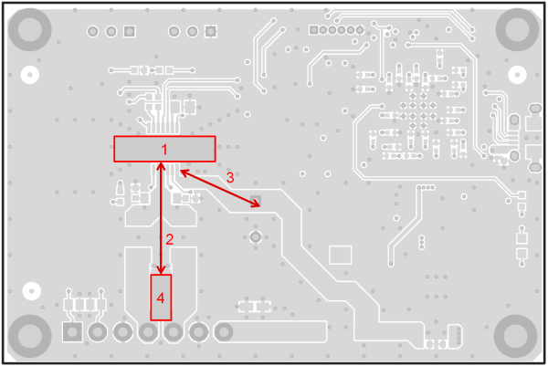
The red boxes around number 1 are the copper ground on the top layer. Soldered directly to the thermal pad, the ground is the first significant thermal dissipation required. There are vias that go to the other layers for further thermal relief, but vias have high thermal resistance. TI recommends that use of the top layer be mostly for thermal dissipation. A further recommendation is short routes from output pins to the second-order LC filter for EMC suppression. The number 2 arrow indicates these short routes for better ECM results. A short route from the PVDD pin to the LC filter from the battery or power source, as indicated by the number 3 arrow, also improves EMC suppression. Route on an outside layer for added current capability. The red box around number 4 indicates the ground plane that is common to both OUTP and OUTN. Place the capacitors of the LC filter in the common ground plane to help with common-mode noise and short ground loops
 Figure 8-2 Top layer