JAJSVI1 October 2024 TPS25763-Q1
PRODUCTION DATA
- 1
- 1 特長
- 2 アプリケーション
- 3 概要
- 4 Device Comparison Table
- 5 Pin Configuration and Functions
-
6 Specifications
- 6.1 Absolute Maximum Ratings
- 6.2 ESD Ratings
- 6.3 Recommended Operating Conditions
- 6.4 Recommended Components
- 6.5 Thermal Information
- 6.6 Buck-Boost Regulator
- 6.7 CC Cable Detection Parameters
- 6.8 CC VCONN Parameters
- 6.9 CC PHY Parameters
- 6.10 Thermal Shutdown Characteristics
- 6.11 Oscillator Characteristics
- 6.12 ADC Characteristics
- 6.13 TVSP Parameters
- 6.14 Input/Output (I/O) Characteristics
- 6.15 BC1.2 Characteristics
- 6.16 I2C Requirements and Characteristics
- 6.17 Typical Characteristics
- 7 Parameter Measurement Information
-
8 Detailed Description
- 8.1 Overview
- 8.2 Functional Block Diagram
- 8.3
Feature Description
- 8.3.1 Device Power Management and Supervisory Circuitry
- 8.3.2 TVSP Device Configuration and ESD Protection
- 8.3.3 External NFET and LSGD
- 8.3.4
Buck-Boost Regulator
- 8.3.4.1 Buck-Boost Regulator Operation
- 8.3.4.2 Switching Frequency, Frequency Dither, Phase-Shift and Synchronization
- 8.3.4.3 VIN Supply and VIN Over-Voltage Protection
- 8.3.4.4 Feedback Paths and Error Amplifiers
- 8.3.4.5 Transconductors and Compensation
- 8.3.4.6 Output Voltage DAC, Soft-Start and Cable Droop Compensation
- 8.3.4.7 VBUS Overvoltage Protection
- 8.3.4.8 VBUS Undervoltage Protection
- 8.3.4.9 Current Sense Resistor (RSNS) and Current Limit Operation
- 8.3.4.10 Buck-Boost Peak Current Limits
- 8.3.5 USB-PD Physical Layer
- 8.3.6 VCONN
- 8.3.7 Cable Plug and Orientation Detection
- 8.3.8 ADC
- 8.3.9 BC 1.2, Legacy and Fast Charging Modes (Px_DP, Px_DM)
- 8.3.10 DisplayPort Hot-Plug Detect (HPD)
- 8.3.11 USB2.0 Low-Speed Endpoint
- 8.3.12 Digital Interfaces
- 8.3.13 I2C Interface
- 8.3.14 Digital Core
- 8.3.15 NTC Input
- 8.3.16 Thermal Sensors and Thermal Shutdown
- 8.4 Device Functional Modes
- 9 Application and Implementation
- 10Device and Documentation Support
- 11Revision History
- 12Mechanical, Packaging, and Orderable Information
8.3.4.1 Buck-Boost Regulator Operation
The TPS25763-Q1 devices utilize a fixed frequency, current mode control buck-boost converter. This converter operates in forced continuous conduction mode (CCM) and therefore allows inductor current to flow in either direction at light loads. The power train consists of five N-Channel power MOSFETs. See Figure 8-8. Transistors M1 and M2 are the high-side and low-side buck FETs. Transistors M3 and M4 are the high-side and low-side boost FETs. Transistor M5 blocks reverse conduction from OUT to SW2 during input overvoltage transients as explained in VIN Supply and VIN Over-Voltage Protection.
- IN: Receives power from the battery. The input bulk capacitor must be connected between IN and PGND.
- OUT: Delivers power from the switching converter. The output bulk capacitor connects between OUT to PGND.
- PGND: Ground return for the switching converter power train.
- AGND: Ground return for everything except the power train. The voltage feedback divider returns to AGND. PGND and AGND must connect together on the circuit board.
- LDO_5V: Provides gate drive for M2 and M4 and current for the bootstrap circuits feeding BOOT1 and BOOT2. A bypass capacitor must connect from LDO_5V to PGND. See Internal LDO Regulators for more information on LDO_5V.
- LDO_3V3: Analog circuitry power supply. A bypass capacitor must connect from LDO_3V3 to AGND. See Internal LDO Regulators for more information on LDO_3V3.
- BOOT1: Provides gate drive for M1. A bootstrap capacitor must connect from BOOT1 to SW1.
- BOOT2: Provides gate drive for M3. A bootstrap capacitor must connect from BOOT2 to SW2.
- SW1: Connects M1 and M2 to external inductor.
- SW2: Connects M3 and M4 to external inductor.
- CSP: Positive terminal of average current sense amplifier. Connects to positive terminal of output bulk capacitor.
- CSN/BUS: Negative terminal of average current sense amplifier. A 10-mΩ current sense resistor is externally connected from CSP to CSN/BUS.
Depending upon the input voltage VIN and the output voltage VOUT, the converter can operate in one of four different states, each of which is described in following sections.
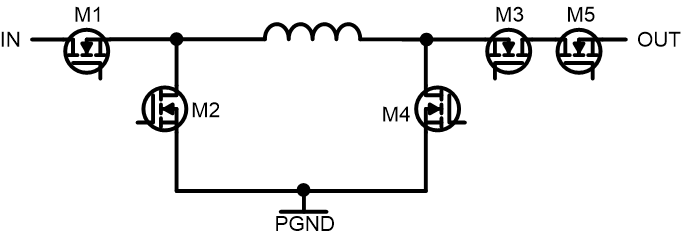 Figure 8-8 Buck-Boost Internal Power
FETs
Figure 8-8 Buck-Boost Internal Power
FETsBuck State
When the input voltage VIN significantly exceeds the output voltage VOUT, the converter enters the buck region of operation in which it performs an endless series of buck switching cycles Buck State. M3 and M5 are constantly on and M4 is constantly off. When the clock signals that a switching cycle has begun, the controller turns on M2 and turns off M1. This switch configuration corresponds to the off-time interval of a traditional buck converter. The voltage difference VSW1 – VSW2 across the inductor equals –VOUT. The inductor current IL ramps down until it reaches a threshold IVALLEY set by the error amplifiers. The controller then turns off M2 and turns on M1. This switch configuration corresponds to the on-time interval of a traditional buck converter. The voltage difference VSW1 – VSW2 now equals VIN – VOUT. The inductor current now ramps up until the converter clock signals that the end of the switching cycle has been reached.
The on-time ton equals the time interval during which M1 conducts. The off-time toff equals the time interval during which M2 conducts. Because the converter operates in FCCM, the period τ equals the sum of ton and toff. During the buck state, the controller regulates power flow by adjusting the buck duty cycle D, which equals the ratio ton/τ.
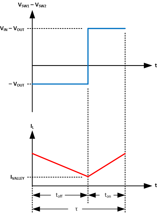 Figure 8-9 Buck State
Buck Transition State
When the input voltage VIN is only slightly larger than the output voltage VOUT, the converter enters the buck transition region of operation in which it alternately performs buck and boost switching cycles Buck Transition. M5 is always on. When the clock signals that a buck switching cycle has begun, the controller turns on M2 and M3, and it turns off M1 and M4. This switch configuration corresponds to the off-time of a traditional buck converter. The inductor current IL ramps down until it reaches a threshold IVALLEY set by the error amplifiers. The controller then turns off M2 and turns on M1. This switch configuration corresponds to the on-time of a traditional buck converter. The inductor current now ramps up slowly until the clock signals the end of the buck switching cycle. The next switching cycle is a boost switching cycle. When this cycle begins, the controller turns M3 off and turns M4 on. M2 remains off, and both M1 and M5 remain on. This switch configuration corresponds to the on-time of a traditional boost converter. The inductor current IL now ramps up rapidly until the fixed on-time expires. The controller then turns off M4 and turns on M3. The inductor current now ramps down until the clock signals the end of the boost switching cycle. The next switching cycle is another buck cycle.
During the buck transition state, the controller regulates power flow by adjusting the buck duty cycle. The boost duty cycle remains fixed. If the converter remains in the buck state rather than move to the buck transition state, the buck on-time becomes so short that it is impossible to regulate power flow without pulse skipping.
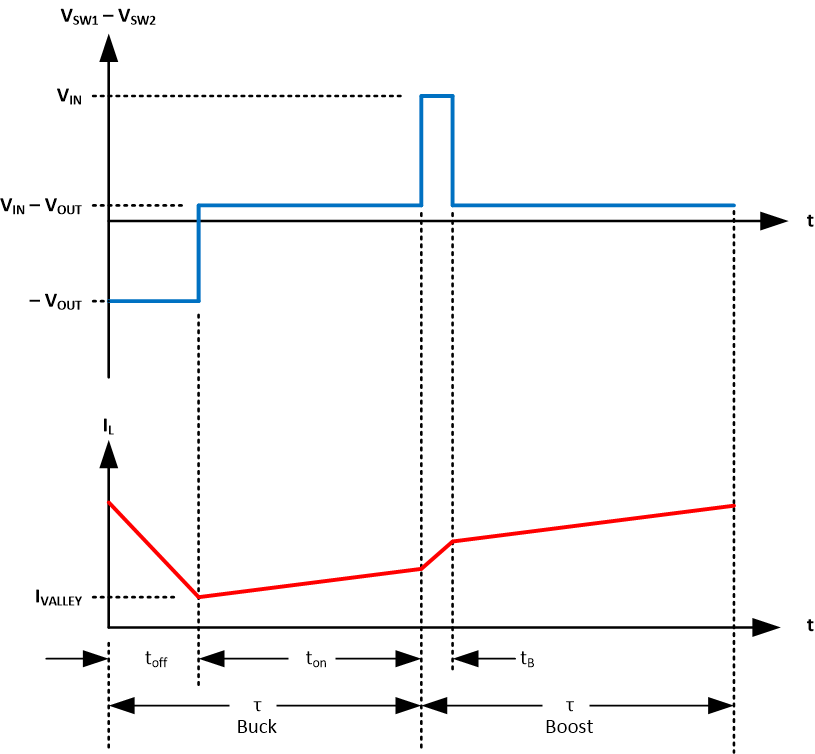 Figure 8-10 Buck Transition
Boost Transition State
When the input voltage VIN is only slightly smaller than the output voltage VOUT, the converter enters the boost transition region of operation in which it alternately performs boost and buck switching cycles Boost Transition. M5 is always on. When the clock signals that a boost switching cycle has begun, the controller turns on M1 and M4, and it turns off M2 and M3. This switch configuration corresponds to the on-time of a traditional boost converter. The inductor current IL ramps up until it reaches a threshold IPEAK set by the error amplifiers. The controller then turns off M4 and turns on M3. This switch configuration corresponds to the off-time of a traditional boost converter. The inductor current now ramps down slowly until the clock signals the end of the boost switching cycle. The next switching cycle is a buck switching cycle. When this cycle begins, the controller turns M1 off and turns M2 on. M4 remains off, and both M3 and M5 remain on. This switch configuration corresponds to the off-time of a traditional buck converter. The inductor current IL now ramps down rapidly until the fixed off-time expires. The controller then turns off M2 and turns on M1. The inductor current now ramps up until the clock signals the end of the buck switching cycle. The next switching cycle is another boost cycle.
During the boost transition state, the controller regulates power flow by adjusting the boost duty cycle. The buck duty cycle remains fixed. If the converter remains in the boost state rather than move to the boost transition state, the boost on-time is so short that it is impossible to regulate power flow without pulse skipping.
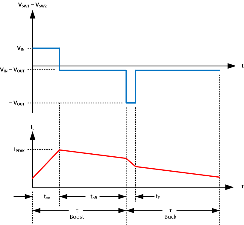 Figure 8-11 Boost Transition
Boost State
When the input voltage VIN is significantly less than the output voltage VOUT, the converter enters the boost region of operation in which it performs an endless series of boost switching cycles Boost State. M1 and M5 are constantly on and M2 is constantly off. When the clock signals that a switching cycle has begun, the controller turns on M4 and turns off M3. This switch configuration corresponds to the on-time interval of a traditional boost converter. The voltage difference VSW1 – VSW2 across the inductor equals VIN. The inductor current IL ramps up until it reaches a threshold IPEAK set by the error amplifiers. The controller then turns off M4 and turns on M3. This switch configuration corresponds to the off-time interval of a traditional boost converter. The voltage difference VSW1 – VSW2 now equals VIN – VOUT, which is negative. The inductor current now ramps down until the converter clock signals that the end of the switching cycle has been reached.
The on-time ton equals the time interval during which M4 conducts. The off-time toff equals the time interval during which M3 conducts. Because the converter operates in FCCM, the period τ equals the sum of ton and toff. During the boost state, the controller regulates power flow by adjusting the boost duty cycle D, which equals the ratio ton/τ.
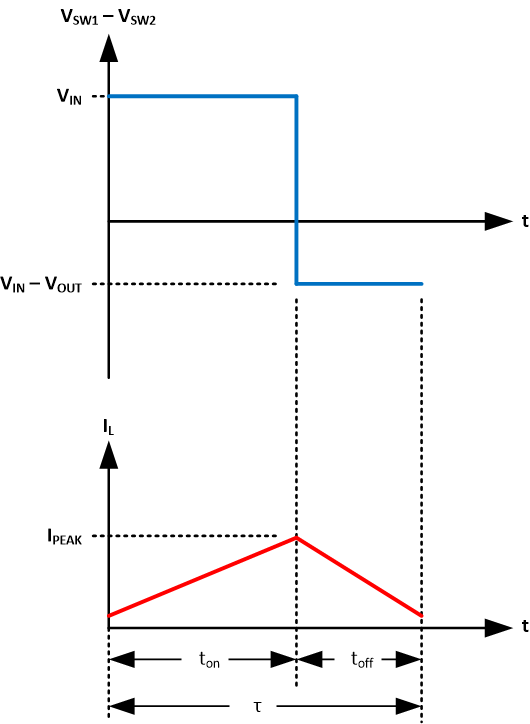 Figure 8-12 Boost State
Boundaries of the Regions of Operation
Regions of Operation graphically depicts the four regions of operation and the boundaries between them. When VBUS > kVIN, the converter remains in the boost region of operation. The value k is 1.2. When VIN < VBUS < kVIN, the converter enters the boost transition region of operation. When VIN/k < VBUS < VIN, the converter enters the buck transition region of operation. When VBUS < VIN/k, the converter enters the buck region of operation. The converter ceases operating if VIN exceeds the OVP threshold, which lies between 18 and 20 V. Similarly, the converter also ceases operating if VIN drops below either the internal UVLO threshold, which lies between 5 and 5.5 V, or the user programmed EN/UVLO threshold (see VIN UVLO and ENABLE/UVLO, whichever is greater).
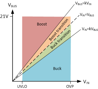 Figure 8-13 Regions of Operation