JAJSVO0 November   2024 LMR51603

PRODUCTION DATA  

  1.   1
  2. 特長
  3. アプリケーション
  4. 概要
  5. Device Comparison Table
  6. Pin Configuration and Functions
  7. Specifications
    1. 6.1 Absolute Maximum Ratings
    2. 6.2 ESD Ratings
    3. 6.3 Recommended Operating Conditions
    4. 6.4 Thermal Information
    5. 6.5 Electrical Characteristics
    6. 6.6 Typical Characteristics
  8. Detailed Description
    1. 7.1 Overview
    2. 7.2 Functional Block Diagram
    3. 7.3 Feature Description
      1. 7.3.1 Fixed Frequency Peak Current Mode Control
      2. 7.3.2 Adjustable Output Voltage
      3. 7.3.3 Enable
      4. 7.3.4 Minimum ON Time, Minimum OFF Time, and Frequency Foldback
      5. 7.3.5 Bootstrap Voltage
      6. 7.3.6 Overcurrent and Short-Circuit Protection
      7. 7.3.7 Soft Start
      8. 7.3.8 Thermal Shutdown
    4. 7.4 Device Functional Modes
      1. 7.4.1 Shutdown Mode
      2. 7.4.2 Active Mode
      3. 7.4.3 CCM Mode
      4. 7.4.4 Light Load Operation (PFM Version)
      5. 7.4.5 Light-Load Operation (FPWM Version)
  9. Application and Implementation
    1. 8.1 Application Information
    2. 8.2 Typical Application
      1. 8.2.1 Design Requirements
      2. 8.2.2 Detailed Design Procedure
        1. 8.2.2.1 Custom Design With WEBENCH® Tools
        2. 8.2.2.2 Output Voltage Setpoint
        3. 8.2.2.3 Switching Frequency
        4. 8.2.2.4 Inductor Selection
        5. 8.2.2.5 Output Capacitor Selection
        6. 8.2.2.6 Input Capacitor Selection
        7. 8.2.2.7 Bootstrap Capacitor
        8. 8.2.2.8 Undervoltage Lockout Setpoint
        9. 8.2.2.9 Replacing Non-Sync Buck Converter
      3. 8.2.3 Application Curves
    3. 8.3 Power Supply Recommendations
    4. 8.4 Layout
      1. 8.4.1 Layout Guidelines
        1. 8.4.1.1 Compact Layout for EMI Reduction
        2. 8.4.1.2 Feedback Resistors
      2. 8.4.2 Layout Example
  10. Device and Documentation Support
    1. 9.1 Device Support
      1. 9.1.1 サード・パーティ製品に関する免責事項
      2. 9.1.2 Development Support
        1. 9.1.2.1 Custom Design With WEBENCH® Tools
    2. 9.2 Documentation Support
      1. 9.2.1 Related Documentation
    3. 9.3 ドキュメントの更新通知を受け取る方法
    4. 9.4 サポート・リソース
    5. 9.5 Trademarks
    6. 9.6 静電気放電に関する注意事項
    7. 9.7 用語集
  11. 10Revision History
  12. 11Mechanical, Packaging, and Orderable Information

Typical Characteristics

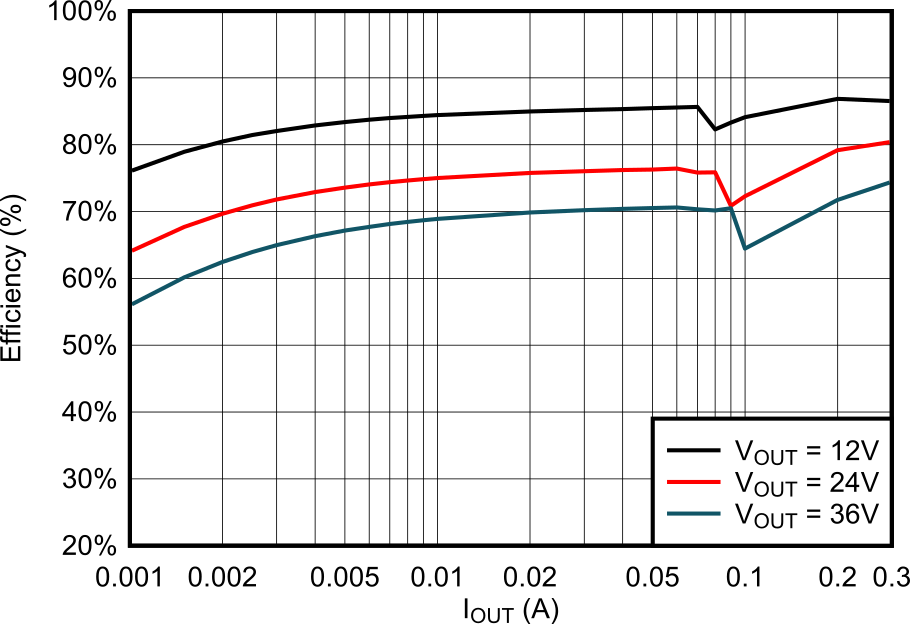
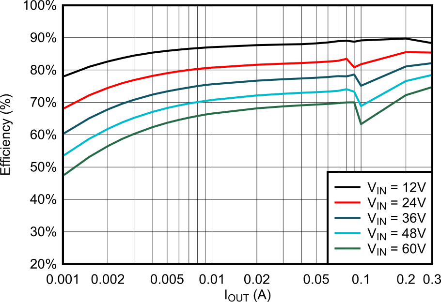
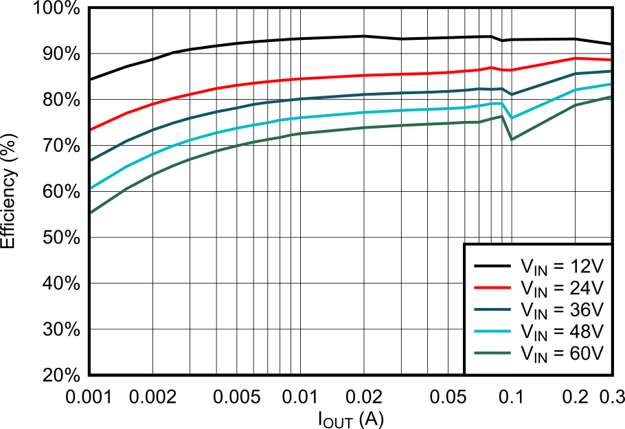
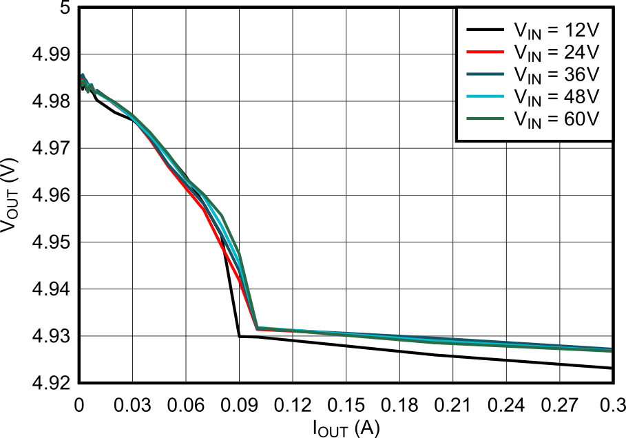
VIN = 24V, fSW= 400kHz, TA = 25°C, unless otherwise specified.
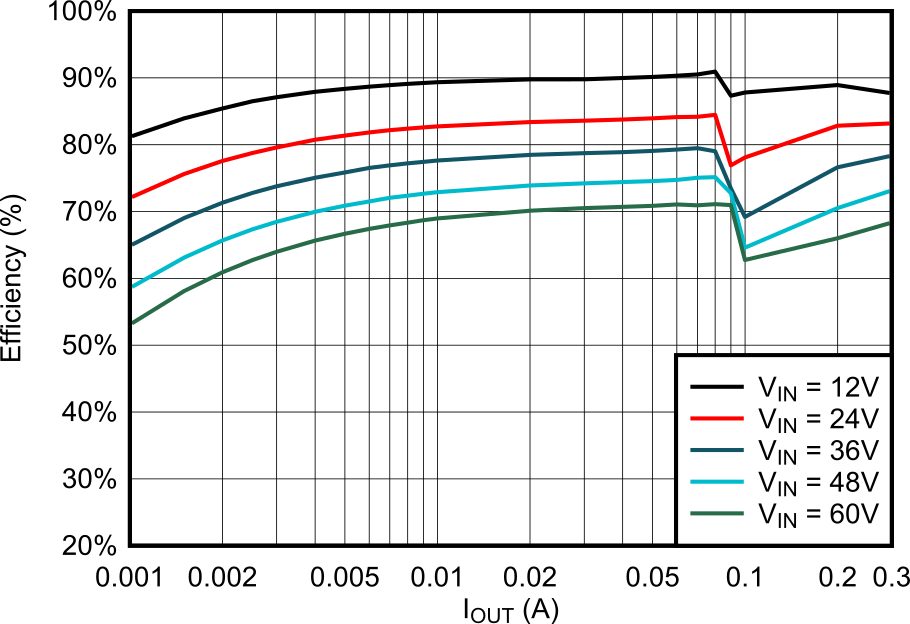
LMR51603 5V PFM Efficiency vs Load Current
fSW = 1100kHzVOUT = 5VLMR51603Y
Figure 6-1 5V PFM Efficiency vs Load Current
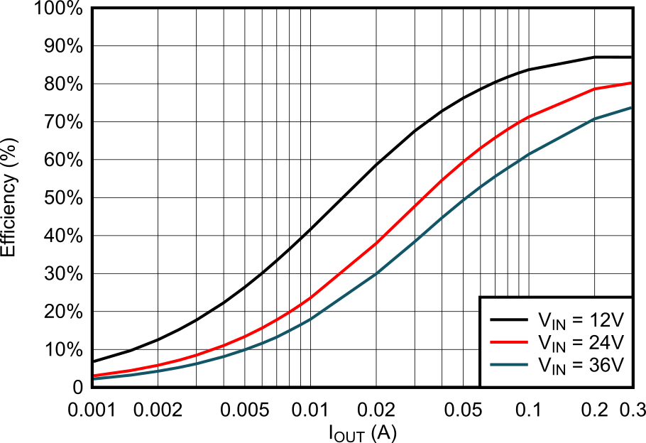
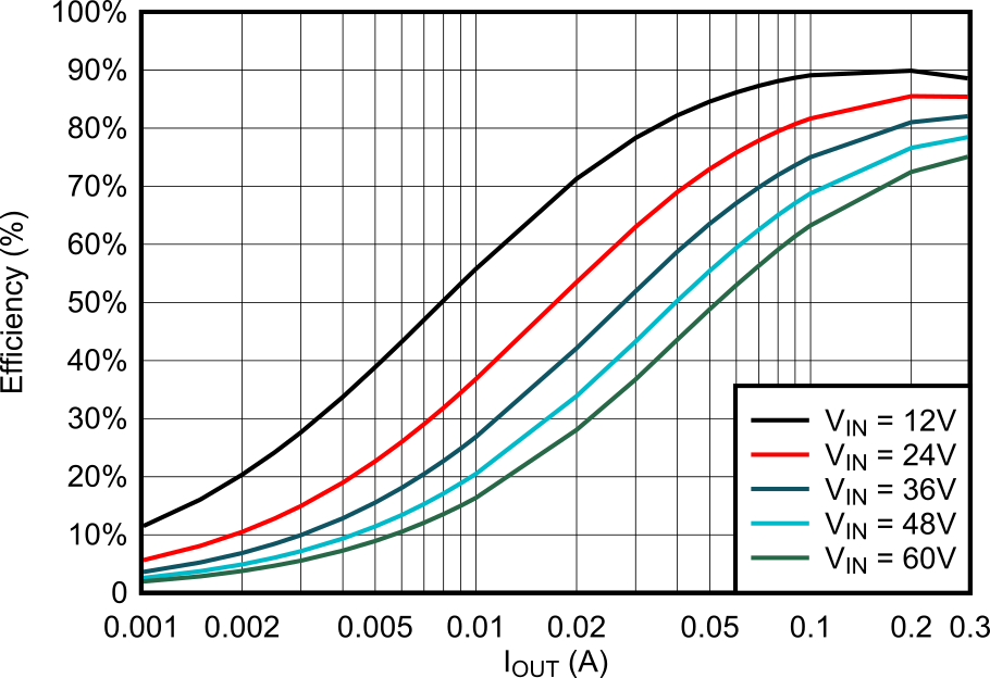
LMR51603 3.3V PFM Efficiency vs Load Current
fSW = 1100kHzVOUT = 3.3VLMR51603Y
Figure 6-3 3.3V PFM Efficiency vs Load Current
LMR51603 3.3V PFM Efficiency vs Load Current
fSW = 400kHzVOUT = 3.3VLMR51603X
Figure 6-5 3.3V PFM Efficiency vs Load Current
LMR51603 5V PFM Efficiency vs Load Current
fSW = 400kHzVOUT = 5VLMR51603X
Figure 6-7 5V PFM Efficiency vs Load Current
LMR51603 5V load Regulation
fSW = 400kHzVOUT = 5VLMR51603X
Figure 6-9 5V load Regulation
LMR51603 VIN Quiescent Current vs TemperatureFigure 6-11 VIN Quiescent Current vs Temperature
LMR51603 Reference Voltage vs TemperatureFigure 6-13 Reference Voltage vs Temperature
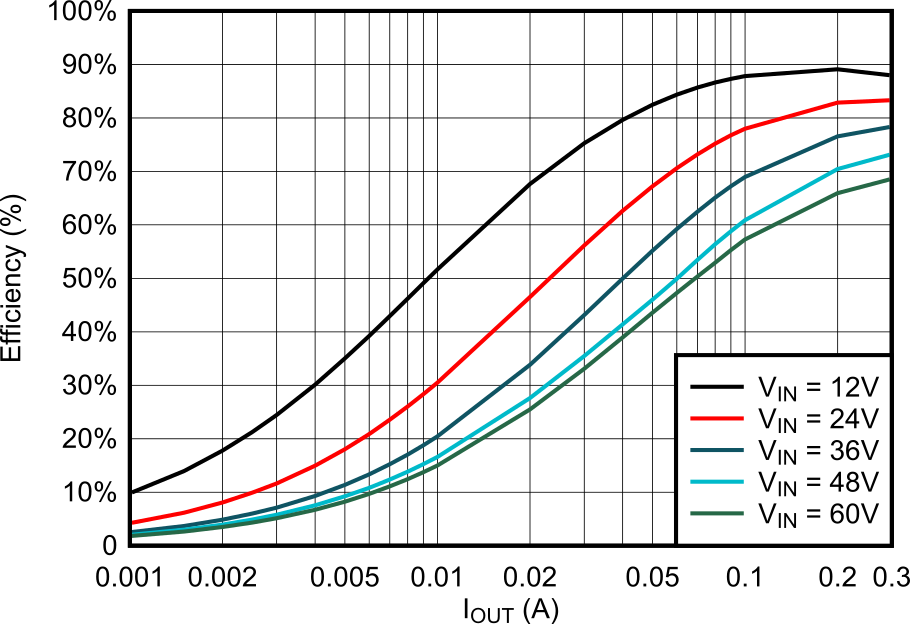
LMR51603 5V FPWM Efficiency vs Load Current
fSW =1100kHzVOUT = 5VLMR51603YF
Figure 6-2 5V FPWM Efficiency vs Load Current
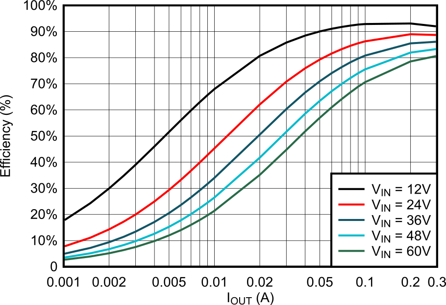
LMR51603 3.3V FPWM Efficiency vs Load Current
fSW =1100kHzVOUT = 3.3VLMR51603YF
Figure 6-4 3.3V FPWM Efficiency vs Load Current
LMR51603 3.3V FPWM Efficiency vs Load Current
fSW = 400kHzVOUT = 3.3VLMR51603XF
Figure 6-6 3.3V FPWM Efficiency vs Load Current
LMR51603 5V FPWM Efficiency vs Load Current
fSW = 400kHzVOUT = 5VLMR51603XF
Figure 6-8 5V FPWM Efficiency vs Load Current
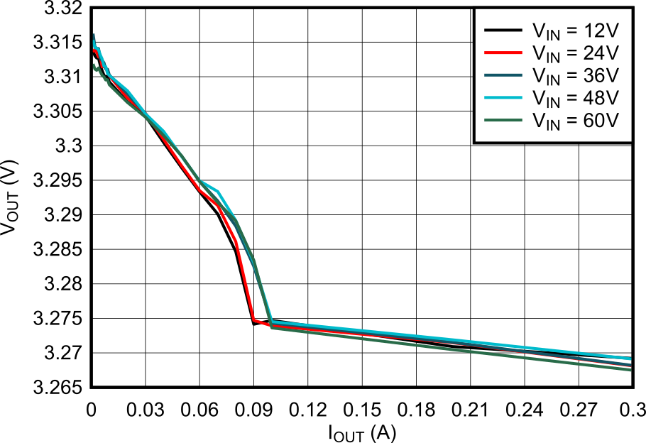
LMR51603 3.3V Load Regulation
fSW = 400kHzVOUT = 3.3VLMR51603X
Figure 6-10 3.3V Load Regulation
LMR51603 VIN UVLO vs TemperatureFigure 6-12 VIN UVLO vs Temperature
LMR51603 HS and LS Current Limit vs TemperatureFigure 6-14 HS and LS Current Limit vs Temperature