JAJSVQ6 November   2024 DRV81004-Q1

ADVANCE INFORMATION  

  1.   1
  2. 特長
  3. アプリケーション
  4. 概要
  5. Pin Configuration and Functions
  6. Specifications
    1. 5.1 Absolute Maximum Ratings
    2. 5.2 ESD Ratings
    3. 5.3 Recommended Operating Conditions
    4. 5.4 Thermal Information
    5. 5.5 Electrical Characteristics
      1. 5.5.1 SPI Timing Requirements
  7. Detailed Description
    1. 6.1 Overview
    2. 6.2 Functional Block Diagram
    3. 6.3 Feature Description
      1. 6.3.1 Control Pins
        1. 6.3.1.1 Input Pins
        2. 6.3.1.2 nSLEEP Pin
      2. 6.3.2 Power Supply
        1. 6.3.2.1 Modes of Operation
          1. 6.3.2.1.1 Power-up
          2. 6.3.2.1.2 Sleep mode
          3. 6.3.2.1.3 Idle mode
          4. 6.3.2.1.4 Active mode
          5. 6.3.2.1.5 Limp Home mode
          6. 6.3.2.1.6 Reset condition
      3. 6.3.3 Power Stage
        1. 6.3.3.1 Switching Resistive Loads
        2. 6.3.3.2 Inductive Output Clamp
        3. 6.3.3.3 Maximum Load Inductance
        4. 6.3.3.4 Switching Channels in parallel
      4. 6.3.4 Protection and Diagnostics
        1. 6.3.4.1 Undervoltage on VM
        2. 6.3.4.2 Overcurrent Protection
        3. 6.3.4.3 Over Temperature Protection
        4. 6.3.4.4 Over Temperature Warning
        5. 6.3.4.5 Over Temperature and Overcurrent Protection in Limp Home mode
        6. 6.3.4.6 Reverse Polarity Protection
        7. 6.3.4.7 Over Voltage Protection
        8. 6.3.4.8 Output Status Monitor
      5. 6.3.5 SPI Communication
        1. 6.3.5.1 SPI Signal Description
          1. 6.3.5.1.1 Chip Select (nSCS)
            1. 6.3.5.1.1.1 Logic high to logic low Transition
            2. 6.3.5.1.1.2 Logic low to logic high Transition
          2. 6.3.5.1.2 Serial Clock (SCLK)
          3. 6.3.5.1.3 Serial Input (SDI)
          4. 6.3.5.1.4 Serial Output (SDO)
        2. 6.3.5.2 Daisy Chain Capability
        3. 6.3.5.3 SPI Protocol
        4. 6.3.5.4 SPI Registers
          1. 6.3.5.4.1  Standard Diagnosis Register
          2. 6.3.5.4.2  Output control register
          3. 6.3.5.4.3  Input 0 Mapping Register
          4. 6.3.5.4.4  Input 1 Mapping Register
          5. 6.3.5.4.5  Input Status Monitor Register
          6. 6.3.5.4.6  Open Load Current Control Register
          7. 6.3.5.4.7  Output Status Monitor Register
          8. 6.3.5.4.8  Configuration Register
          9. 6.3.5.4.9  Output Clear Latch Register
          10. 6.3.5.4.10 Configuration Register 2
  8. Application and Implementation
    1. 7.1 Application Information
      1. 7.1.1 Typical Application
      2. 7.1.2 Suggested External Components
    2. 7.2 Layout
      1. 7.2.1 Layout Guidelines
      2. 7.2.2 Package Footprint Compatibility
  9. Device and Documentation Support
    1. 8.1 ドキュメントの更新通知を受け取る方法
    2. 8.2 サポート・リソース
    3. 8.3 Trademarks
    4. 8.4 静電気放電に関する注意事項
    5. 8.5 用語集
  10. Revision History
  11. 10Mechanical, Packaging, and Orderable Information

Package Footprint Compatibility

The PWP0014L package of the DRV81004-Q1 is footprint compatible with other SO-14 packages used in the industry, as shown in Figure 7-2 and Figure 7-3.
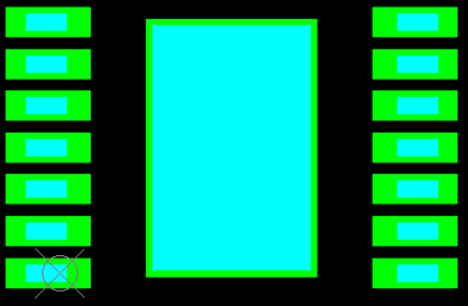
DRV81004-Q1 PWP0014L on another SO-14 PCB Pad, Light blue: TI PWP0014L leads, Green: Other SO-14 PCB PadFigure 7-2 PWP0014L on another SO-14 PCB Pad, Light blue: TI PWP0014L leads, Green: Other SO-14 PCB Pad
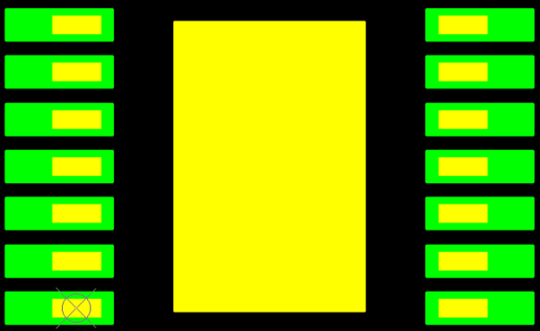
DRV81004-Q1 SO-14 on PWP0014L PCB Pad, Yellow: Other SO-14 leads, Green: TI PWP0014L PCB PadFigure 7-3 SO-14 on PWP0014L PCB Pad, Yellow: Other SO-14 leads, Green: TI PWP0014L PCB Pad