JAJU835 December 2021
- 概要
- リソース
- 特長
- アプリケーション
- 5
- 1System Description
-
2System Overview
- 2.1 Block Diagram
- 2.2 Highlighted Products
- 2.3
Design Considerations
- 2.3.1
Design Hardware Implementation
- 2.3.1.1 Hall-Effect Switches
- 2.3.1.2 Linear Hall-Effect Sensor Output
- 2.3.1.3 Power Supply
- 2.3.1.4 Transistor Circuit for Creating High-Voltage Enable Signal
- 2.3.2 Alternative Implementations
- 2.3.1
Design Hardware Implementation
- 3Hardware, Software, Testing Requirements, and Test Results
- 4Design and Documentation Support
3.1.1 Installation and Demonstration Instructions
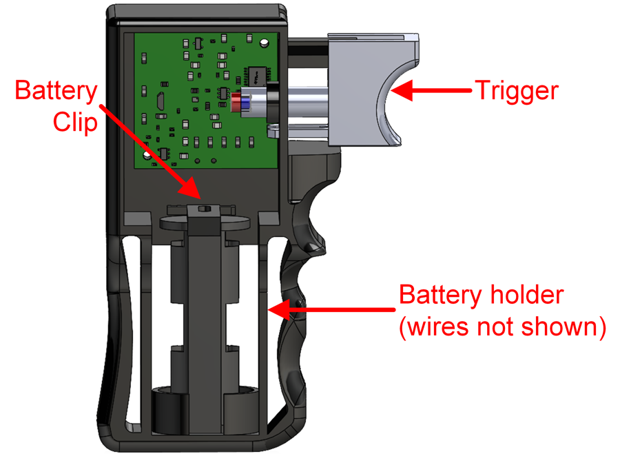
This hardware comes with an empty battery holder that is placed inside the 3D printed trigger module. Figure 3-1 shows the 3D model of the trigger module (note that the spring and the battery holder wires are not shown in the image).
 Figure 3-1 Front View With Battery Holder
Inside Trigger Module
Figure 3-1 Front View With Battery Holder
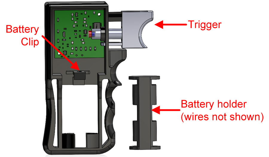
Inside Trigger ModuleTo use this design, batteries must be placed inside the battery holder. Batteries can be installed by first pushing the battery clip upwards and simultaneously taking the battery holder outside of the trigger module. Figure 3-2 shows a 3D model with the battery holder placed outside the trigger module. After the battery holder is outside the trigger module, install the two AAA batteries into the battery holder. Finally, the battery holder should be placed back into the trigger module by pressing the clip upwards while placing the battery holder back into the trigger module until the battery holder is inside the trigger module again (see Figure 3-1).
 Figure 3-2 Front View With Battery Holder
Outside Trigger Module
Figure 3-2 Front View With Battery Holder
Outside Trigger ModuleThe design can be used in standalone mode by pressing the trigger in Figure 3-1 to the left and observing the state of the LEDs on the board. When the trigger displacement reaches a certain distance threshold, the system is awakened from sleep mode. LEDs D1, D2, and LPWR will be ON when the system is in active mode and LEDs D3 and D4 will be OFF. In addition, the TRIG LED will change its brightness based on how far the trigger is pressed. The further the trigger is pressed, the brighter the TRIG LED will appear. Note that the trigger cannot be pressed to reach a full displacement distance of 10 mm due to the spring preventing the trigger from being fully pressed.
If an external magnetic field is detected by switch U3, LED U3 will be on and the system will be placed in sleep mode. Similarly, if an external magnetic field is detected by switch U4, LED U4 will be turned ON and the system will also be placed in sleep mode. As an alternative to viewing the state of the LED, the outputs of the different Hall sensors can also be observed by measuring the output voltage at the corresponding test points on the board. Section 3.1.2 provides more details on the test points and LEDs available on this board.