JAJU848 April 2022 TPSI3050 , TPSI3050-Q1 , TPSI3052 , TPSI3052-Q1
2.3 Design Considerations
The TPSI3050-Q1 is a fully integrated, isolated switch driver, which when combined with an external power switch, forms a complete isolated solid-state relay (SSR) solution. With a nominal gate drive voltage of 10 V and 1.5/3.0 A peak source and sink current, a large variety of external power switches can be chosen to meet a wide range of applications. The TPSI3050-Q1 generates its own secondary bias supply from the power received from its primary side, so no isolated secondary supply bias is required. Additionally, the TPSI3050-Q1 can optionally supply power to external supporting circuitry for various application needs. In three-wire mode, the primary supply of 3 V to 5.5 V is supplied externally, and the switch is controlled through a separate enable.
TPSI3050-Q1 features:
- Adjustable power transfer
- Integrated 10-V gate supply
- Up to 50 mW supply to power auxiliary circuitry (IAUX)
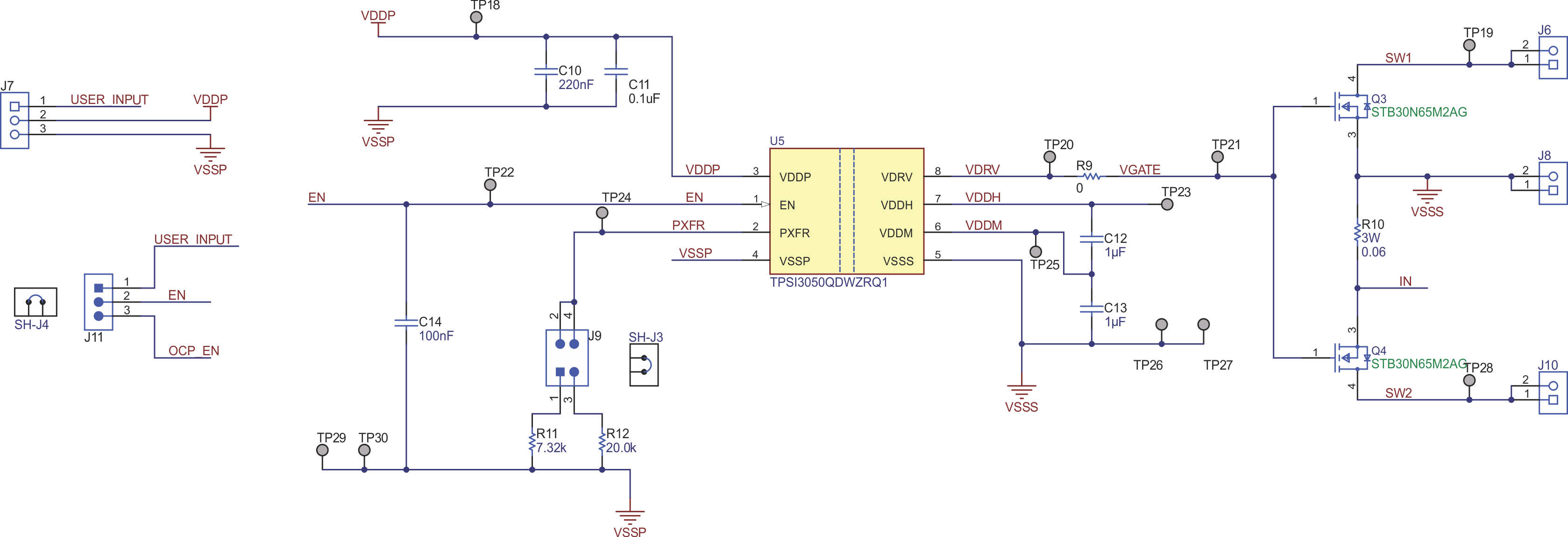
 Figure 2-2 Solid-State Relay
Circuit
Figure 2-2 Solid-State Relay
CircuitFor the primary side, TPSI3050-Q1 is set to three-wire mode configuration to achieve the highest power transfer available. Using a 20 kΩ resistor with a 1 % tolerance in PXFR pin provides the highest power transfer available and supports up to 50 mW of IAUX. It is recommended to add a 1 uF in parallel with a 0.1 uF ceramic capacitor with low ESR to VDDP.
For the secondary side, CDIV1 (C12) and CDIV2 (C13) capacitors need to be properly selected to drive the back to back MOSFETs. If CDIV1 and CDIV2 are too small, then the voltage drop in VDDH will trigger an undervoltage lockout (UVLO) and disable the driver. The following two equations can be used for calculating the proper capacitance values.
- n is a real number greater than or equal to 1.0.
- CDIV1 is the external capacitance from VDDH to VDDM.
- CDIV2 is the external capacitance from VDDM to VSSS.
- QLOAD is the total charge of the load from VDRV to VSSS.
- ΔV is the voltage drop on VDDH when switching the load.
The MOSFETs selected for this design each have a gate charge (QG) of 31 nC. Since the design uses back to back MOSFETs, then the total QG is 62 nC. If CDIV1 = CDIV2= CDIV, then CDIV must be selected with capacitance higher than 124 nF to ensure that VDDH voltage drop is less than 1 V. Use this excel calculator to calculate for capacitors and power transfer selection. For this design a 1 uF capacitor was selected to have a VDDH voltage drop of 0.124 V.