JAJU848 April 2022 TPSI3050 , TPSI3050-Q1 , TPSI3052 , TPSI3052-Q1
3.2 Test Setup
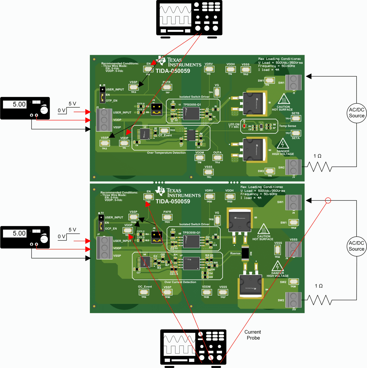
To test the overcurrent protection reference design it is recommended to connect an oscilloscope to EN (enable), OC Event (output of the isolated comparator AMC23C14), and a differential probe to the AC source. Connect a 5 V power source and ensure that the TPSI3050-Q1 has powered up by measuring VDDH (10 V) and VDDM (5 V). Finally, connect the AC or DC source and the load to test the design.
To test the overtemperature protection reference design it is recommended to connect an oscilloscope to EN (enable), OT Event (output of the digital isolator), and a differential probe to the AC source. Connect a 5 V power source and ensure that the TPSI3050-Q1 has powered up by measuring VDDH (10 V) and VDDM (5 V). Finally, connect the AC or DC source and the load to tests the design.
The circuit should look as Figure 3-1.
| Name | Description | |
|---|---|---|
| J1, J6, TP2, TP19 | SW1 | AC/DC source connection |
| J2, J7 | USER_INPUT | External signal to control TPSI3050-Q1 EN signal |
| VDDP | Power supply for primary side | |
| VSSP | Ground supply for primary side | |
| J3, J9 | Power transfer selection | |
| J4, J10, TP9, TP28 | SW2 | Load connection |
| J5 | USER_INPUT | External signal to control TPSI3050-Q1 EN signal without overtemperature protection |
| EN | TPSI3050-Q1 Active high driver enable | |
| OTP_EN | Overtemperature enable signal to control TPSI3050-Q1 | |
| J11 | USER_INPUT | External signal to control TPSI3050-Q1 EN signal without overcurrent protection |
| EN | TPSI3050-Q1 Active high driver enable | |
| OCP_EN | Overcurrent enable signal to control TPSI3050-Q1 | |
| TP1, TP18 | VDDP | TPSI3050-Q1 Power supply for primary side |
| TP3, TP20 | VDRV | TPSI3050-Q1 Active high driver output |
| TP4, TP21 | VG | Gate voltage of the power switches |
| TP5, TP22 | EN | TPSI3050-Q1 Active high driver enable |
| TP6, TP23 | VDDH | TPSI3050-Q1 Generated high supply |
| TP7, TP24 | PXFR | TPSI3050-Q1 Increase or decrease power transfer |
| TP8, TP25 | VDDM | TPSI3050-Q1 Generated mid supply |
| J8, TP10, TP11, TP26, TP27 | VSSS | Ground supply for secondary side |
| TP12, TP13, TP29, TP30 | VSSP | Ground supply for primary side |
| TP14 | SETB | Temperature sensor debug input |
| TP15 | OT_EVENT | Active high signal that is pull down when overtemperature event above 90 °C occurs. |
| TP16 | OUTA | Output of the temperature sensor |
| TP17 | SETA | Temperature sensor debug input |
| TP31 | OC_EVENT | Active high signal that is pull down when overcurrent event above 2 A occurs. |
Steps to Test the Reference Design:
- J3/J9 Connector should be connecting R3 (20 kΩ). This allows for the highest power transfer.
- J5/J11 Connector should be connecting OTP_EN/OCP_EN to EN. This allows the TPSI3050-Q1 to be controlled by the overtemperature/overcurrent detection logic.
- Connect 5-V supply to VDDP.
- Check that VDDM and VDDH rails are 5-V and 10-V respectively.
- Connect DC source with a load.
- Connect 5-V supply to USER_INPUT
 Figure 3-1 Test Setup