JAJU850 May 2022 TPSI3050 , TPSI3050-Q1 , TPSI3052 , TPSI3052-Q1
3.3 Test Results
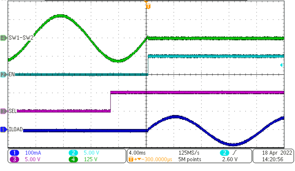
Figure 3-2 shows how the EN signal changes state when the voltage of the AC load reaches the zero voltage point. The SEL signal represents an input signal which signifies that the user is trying to connect the load. The signal does not connect the load immediately because the circuit awaits for the moment when the AC voltage reaches zero. SW1-SW2 is the voltage drop across the back to back MOSFETs and ILOAD is the current on the load. For this design, EN signal is detected at the falling edge of OUT2_CLK using the flip-flop. Once EN is high, TPSI3050-Q1 connects the load. The load remains connected until the user sends a low signal for SEL. This reference design features a immediate load disconnect that allows the user to disconnect the load at any point.
- SW2-SW1 is the voltage drop across the back to back MOSFETs.
- EN is the enable input to TPSI3050-Q1.
- SEL is the input provided by the user when desired to connect the load.
- ILOAD is the current through the load.
 Figure 3-2 Zero-Cross Voltage
Switching
Figure 3-2 Zero-Cross Voltage
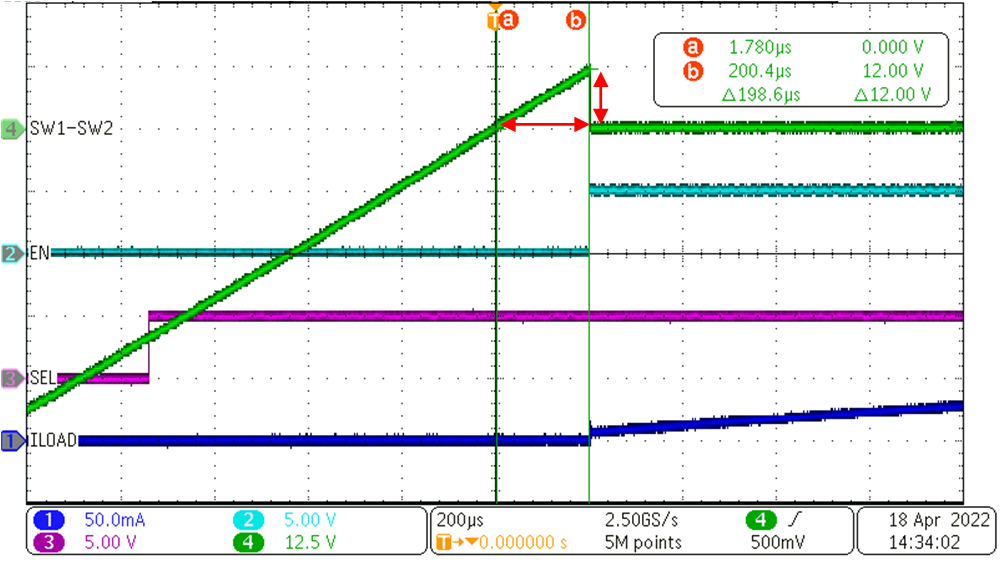
SwitchingFigure 3-3 shows a zoomed in capture of Figure 3-2 to measure the propagation delay and the voltage at which the circuit switches ON. Note that switching ON does not happen right at the zero voltage level and instead it happens at 12 V. This voltage offset is because the input voltage to the isolated comparator has a RC delay constant. This delay is formed by (R4+R5) resistors and the parasitic source-drain capacitance of the power FETs. The voltage level at which the load is connected depends on the value of the bias resistors R4, R5, R7, R8 and the parasitic capacitance of the FETs. The lower the bias resistors values the lower the voltage at which the load is connected. However, there is a important trade off between switching voltage accuracy and the power dissipation across the biasing resistors as previously discussed in section 2.3.
 Figure 3-3 Zero-Cross Voltage Switching
Zoomed