JAJU850 May 2022 TPSI3050 , TPSI3050-Q1 , TPSI3052 , TPSI3052-Q1
2.3.2 AMC23C10
The AMC23C10 is a precision, isolated comparator with short response time that is specifically designed for zero-crossing detection of high-voltage signals that must be galvanically isolated from low-voltage circuitry. The open-drain and push-pull outputs are separated from the input circuitry by an isolation barrier that is highly resistant to magnetic interference. This barrier is certified to provide reinforced galvanic isolation of up to 5 kVRMS according to UL1577, and supports a working voltage of up to 1 kVPK. The device offers an open-drain and a push-pull output with a propagation delay of less than 300 ns. The integrated LDO supports an operating voltage range of 3 V to 27 V on the high-voltage side, allowing the comparator to be powered from a gate-driver supply. The operating voltage range on the low-side is 2.7 V to 5.5 V.
AMC23C10 features:
- Wide high-side supply range: 3 V to 27 V
- Low-side supply range: 2.7 V to 5.5 V
- Trip threshold error: ±6 mV (max)
- Propagation delay: 290 ns (typ)
- High CMTI: 100 kV/μs (min)
- Open-drain and push-pull output
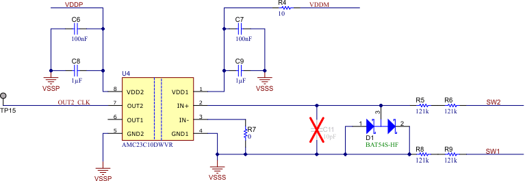
 Figure 2-3 Zero-Cross Detection Circuit
For VDD1 and VDD2, it is recommended to add a 1 uF in parallel with a 0.1 uF ceramic capacitors with low ESR. AMC23C10 is powered on the HV side by TPSI3050-Q1 from the VDDM pin with a 5 V rail. This feature of TPSI3050-Q1 reduces system complexity, cost, and board space.
Figure 2-3 shows IN- input is grounded to effectively compare the voltage swing across the antiparallel diodes D1. Input IN+ is connected to the AC source through R4, R5, R7, and R8. When selecting these resistors it is important to pay attention to the voltage rating, power dissipation and switching delay. The resistors must be able to sustain the high voltage AC source. It is recommended to use resistors in series to meet the voltage specifications. This reference design uses two resistors sized (2010) with a rating of 400V DC. It is important to note the trade-off between the power dissipation across the resistors and the zero voltage detection accuracy. The parasitic capacitance of the power switches and the resistors creates a RC delay for the zero voltage detection. This delay affects the voltage at which zero cross switching happens. Decreasing the resistor value reduces the delay and the load is connected to the source closer to zero volts.
For this design, a resistance of 242 kΩ is used to bias the diodes and achieve zero-cross detection. The AC source is a 110 VAC signal with a 60 Hz frequency. The design connects the load with 180.8 µs delay at 10.4 V. This delay is dominated by the RC constant of (R4+R5) and the output capacitance of the power FETs and not the isolated comparator, the logic circuit on the low side, or the enable delay of the TPSI3050-Q1. Figure 3-3 shows the details of the switching operation. The following equations show the calculation for peak and average power dissipation for the selected resistors. The value R is the addition of the series resistances R = (R4+R5) = (R7+R8).
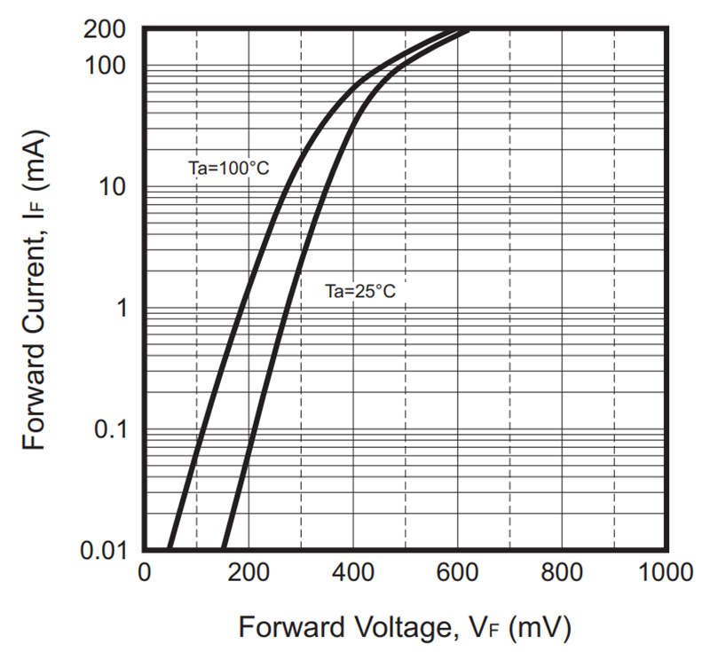
When selecting the series diodes, the voltage drop must higher than the nominal switching threshold voltage for the AMC23C10. AMC23C10 requires a voltage greater than its nominal switching threshold of +/-12.5 mV to detect a valid input. The diode selected for this reference design is a BAT54S-HF. This diode is able to provide the necessary voltage drop at very low current levels. Figure 2-4 shows the forward voltage drop characteristic of BAT54S-HF. Capacitor C11 helps to filter high frequency noises from the AC source, however, C11 can also increase the propagation delay to detect the zero voltage cross. For this design, C11 was not populated in order to maintain lower propagation delay.
 Figure 2-4 Diode Voltage Drop