SBAA525A september 2021 – may 2023 AFE7900 , AFE7920 , AFE7950
1.2.1 ADC to DAC JESD Loopback
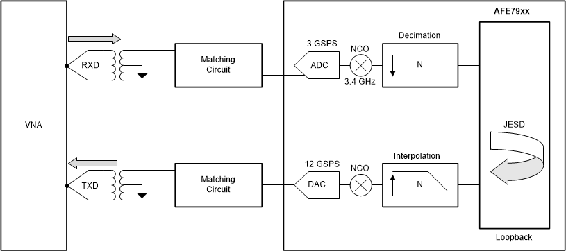
AFE79xx supports internal digital JESD loopback as shown in Figure 1-1 without the need of external STX and SRX lane connection. The internal 20-bit digital stream loopback has been tested by driving RXD using vector network analyzer for gain and group delay parameter plot having 12-GSPS DAC output and multiple JESD data rate from 122.88 MSPS to 491.52 MSPS. The bandwidth is measured across signal tone of 3.4 GHz to demonstrate loopback function for 5G n78 band. The device can also be configured for different frequency bands by tuning external matching circuit accordingly.
 Figure 1-1 ADC to DAC JESD Loopback
Data sheet Switching Characteristics highlights expected latency across different SERDES rates as function of internal clock cycle as shown in Table 1-1.
Overall delay is total latency introduced in signal path due to matching element, RX input to JESD output latency, JESD to TX output latency and internal delay of VNA.
If we take 122.88 MSPS as an example, total internal delay of AFE79xx is 189 clock cycles at 122.88 MHz which approximates to 1.53 us. With external matching elements thus we can achieve sub 2-us group latency response.
| PARAMETER | TEST CONDITIONS | MIN | TYP | MAX | UNIT | ||
|---|---|---|---|---|---|---|---|
| TX CHANNEL LATENCY | |||||||
| SerDes Receiver Analog Delay | Full Rate | 2.8 | ns | ||||
| JESD to TX Ouput Latency | LMFSHd = 2-8-8-1, 368.64 MSPS input rate, 24x Interpolation, Serdes rate = 16.22 Gbps (JESD204C) | 152 | Interface Clock Cycles | ||||
| LMFSHd = 8-16-4-1, 491.52 MSPS input rate, 24x Interpolation, Serdes rate = 16.22 Gbps (JESD204C) | 176 | ||||||
| LMFSHd = 4-16-8-1, 245.76 MSPS input rate, 48x Interpolation, Serdes rate = 16.22 Gbps (JESD204C) | 124 | ||||||
| LMFSHd = 2-16-16-1, 122.88 MSPS input rate, 96x Interpolation, Serdes rate = 16.22 Gbps (JESD204C) | 97 | ||||||
| RX CHANNEL LATENCY | |||||||
| SerDes Transmitter Analog Delay | 3.6 | ns | |||||
| RX Input to JESD Ouput Latency | LMFS = 2-8-8-1, 368.64 MSPS input rate, 8x Decimation, Serdes rate = 16.22 Gbps (JESD204C) | 118 | Interface Clock Cycles | ||||
| LMFS = 2-16-16-1, 122.88 MSPS input rate, 24x Decimation, Serdes rate = 16.22 Gbps (JESD204C) | 92 | ||||||
| LMFS = 4-16-8-1, 245.76 MSPS input rate, 12x Decimation, Serdes rate = 16.22 Gbps (JESD204C) | 108 | ||||||
| LMFS = 4-8-4-1, 491.52 MSPS input rate, 6x Decimation, Serdes rate = 16.22 Gbps (JESD204C) | 153 | ||||||
| FB CHANNEL LATENCY | |||||||
| SerDes Transmitter Analog Delay | 3.6 | ns | |||||
| FB Input to JESD Ouput Latency | LMFS = 1-2-8-1, 368.64 MSPS, 8x Decimation | 151 | Interface Clock Cycles | ||||
| LMFS = 2-4-4-1, 491.52 MSPS, 6x Decimation | 177 | ||||||