SBAS550C June 2011 – May 2015 ADS4229
PRODUCTION DATA.
- 1 Features
- 2 Applications
- 3 Description
- 4 Revision History
- 5 Device Comparison Table
- 6 Pin Configuration and Functions
-
7 Specifications
- 7.1 Absolute Maximum Ratings
- 7.2 ESD Ratings
- 7.3 Recommended Operating Conditions
- 7.4 Thermal Information
- 7.5 Electrical Characteristics: ADS4229 (250 MSPS)
- 7.6 Electrical Characteristics: General
- 7.7 Digital Characteristics
- 7.8 LVDS and CMOS Modes Timing Requirements
- 7.9 LVDS Timings at Lower Sampling Frequencies
- 7.10 CMOS Timings at Lower Sampling Frequencies
- 7.11 Serial Interface Timing Characteristics
- 7.12 Reset Timing (Only when Serial Interface is Used)
- 7.13 Typical Characteristics
-
8 Detailed Description
- 8.1 Overview
- 8.2 Functional Block Diagram
- 8.3 Feature Description
- 8.4 Device Functional Modes
- 8.5 Programming
- 8.6
Register Maps
- 8.6.1 Serial Register Map
- 8.6.2
Description of Serial Registers
- 8.6.2.1 Register Address 00h (Default = 00h)
- 8.6.2.2 Register Address 01h (Default = 00h)
- 8.6.2.3 Register Address 03h (Default = 00h)
- 8.6.2.4 Register Address 25h (Default = 00h)
- 8.6.2.5 Register Address 29h (Default = 00h)
- 8.6.2.6 Register Address 2Bh (Default = 00h)
- 8.6.2.7 Register Address 3Dh (Default = 00h)
- 8.6.2.8 Register Address 3Fh (Default = 00h)
- 8.6.2.9 Register Address 40h (Default = 00h)
- 8.6.2.10 Register Address 41h (Default = 00h)
- 8.6.2.11 Register Address 42h (Default = 00h)
- 8.6.2.12 Register Address 45h (Default = 00h)
- 8.6.2.13 Register Address 4Ah (Default = 00h)
- 8.6.2.14 Register Address 58h (Default = 00h)
- 8.6.2.15 Register Address BFh (Default = 00h)
- 8.6.2.16 Register Address C1h (Default = 00h)
- 8.6.2.17 Register Address CFh (Default = 00h)
- 8.6.2.18 Register Address EFh (Default = 00h)
- 8.6.2.19 Register Address F1h (Default = 00h)
- 8.6.2.20 Register Address F2h (Default = 00h)
- 8.6.2.21 Register Address 2h (Default = 00h)
- 8.6.2.22 Register Address D5h (Default = 00h)
- 8.6.2.23 Register Address D7h (Default = 00h)
- 8.6.2.24 Register Address DBh (Default = 00h)
- 9 Application and Implementation
- 10Power Supply Recommendations
- 11Layout
- 12Device and Documentation Support
- 13Mechanical, Packaging, and Orderable Information
9 Application and Implementation
NOTE
Information in the following applications sections is not part of the TI component specification, and TI does not warrant its accuracy or completeness. TI’s customers are responsible for determining suitability of components for their purposes. Customers should validate and test their design implementation to confirm system functionality.
9.1 Application Information
The ADS4229 dual-channel 12-bit ADC is designed for use in communications receivers designed to receive modern communication signals such as LTE, WIMAX, W-CDMA, and high-order QAM signals. A typical diversity receiver example is shown in Figure 70, where the antennas are placed at some distance to optimize performance in the presence of multipath fading. The path includes a low noise amplifier (LNA), RF mixer, and a digital variable gain amplifier (DVGA). Filtering is used throughout the path to remove blocking signals and mixing products and to prevent aliasing during sampling.
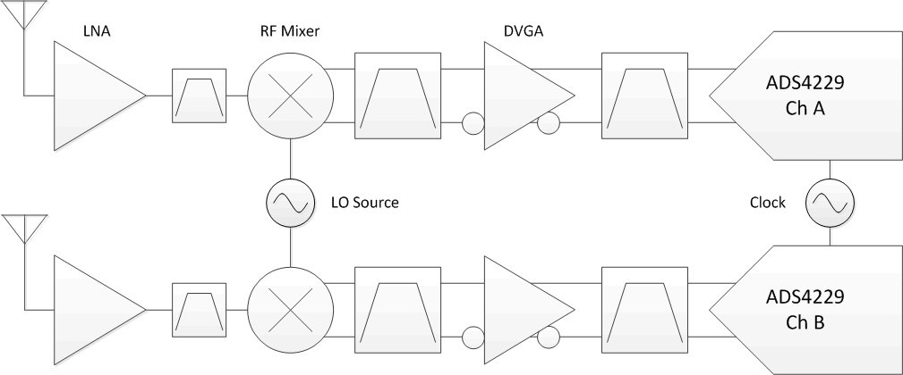 Figure 70. Diversity Communications Receiver
9.1.1 Theory of Operation
At every rising edge of the input clock, the analog input signal of each channel is simultaneously sampled. The sampled signal in each channel is converted by a pipeline of low-resolution stages. In each stage, the sampled/held signal is converted by a high-speed, low-resolution, flash sub-ADC. The difference between the stage input and the quantized equivalent is gained and propagates to the next stage. At every clock, each succeeding stage resolves the sampled input with greater accuracy. The digital outputs from all stages are combined in a digital correction logic block and digitally processed to create the final code after a data latency of 16 clock cycles. The digital output is available as either DDR LVDS or parallel CMOS and coded in either straight offset binary or binary twos complement format. The dynamic offset of the first stage sub-ADC limits the maximum analog input frequency to approximately 400 MHz (with 2-VPP amplitude) or approximately 600 MHz (with 1-VPP amplitude).
9.1.2 Analog Input
The analog input consists of a switched-capacitor-based, differential sample-and-hold (S/H) architecture. This differential topology results in very good ac performance even for high input frequencies at high sampling rates. The INP and INM pins must be externally biased around a common-mode voltage of 0.95 V, available on the VCM pin. For a full-scale differential input, each input pin (INP and INM) must swing symmetrically between
VCM + 0.5 V and VCM – 0.5 V, resulting in a 2-VPP differential input swing. The input sampling circuit has a high 3-dB bandwidth that extends up to 550 MHz (measured from the input pins to the sampled voltage). Figure 71 shows an equivalent circuit for the analog input.
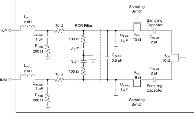 Figure 71. Analog Input Equivalent Circuit
9.1.2.1 Drive Circuit Requirements
For optimum performance, the analog inputs must be driven differentially. This operation improves the common-mode noise immunity and even-order harmonic rejection. A 5-Ω to 15-Ω resistor in series with each input pin is recommended to damp out ringing caused by package parasitics.
SFDR performance can be limited as a result of several reasons, including the effects of sampling glitches; nonlinearity of the sampling circuit; and nonlinearity of the quantizer that follows the sampling circuit. Depending on the input frequency, sample rate, and input amplitude, one of these factors generally plays a dominant part in limiting performance. At very high input frequencies (greater than approximately 300 MHz), SFDR is determined largely by the device sampling circuit nonlinearity. At low input amplitudes, the quantizer nonlinearity usually limits performance.
Glitches are caused by the opening and closing of the sampling switches. The driving circuit should present a low source impedance to absorb these glitches. Otherwise, glitches could limit performance, primarily at low input frequencies (up to approximately 200 MHz). It is also necessary to present low impedance (less than 50 Ω) for the common-mode switching currents. This configuration can be achieved by using two resistors from each input terminated to the common-mode voltage (VCM pin).
The device includes an internal R-C filter from each input to ground. The purpose of this filter is to absorb the sampling glitches inside the device itself. The cutoff frequency of the R-C filter involves a trade-off. A lower cutoff frequency (larger C) absorbs glitches better, but it reduces the input bandwidth. On the other hand, with a higher cutoff frequency (smaller C), bandwidth support is maximized. However, the sampling glitches must then be supplied by the external drive circuit. This tradeoff has limitations as a result of the presence of the package bond-wire inductance.
In the ADS4229, the R-C component values have been optimized while supporting high input bandwidth (up to 550 MHz). However, in applications with input frequencies up to 200 MHz to 300 MHz, the filtering of the glitches can be improved further using an external R-C-R filter; see Figure 74 and Figure 75.
In addition, the drive circuit may have to be designed to provide a low insertion loss over the desired frequency range and matched impedance to the source. Furthermore, the ADC input impedance must be considered. Figure 72 and Figure 73 show the impedance (ZIN = RIN || CIN) looking into the ADC input pins.
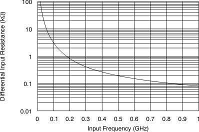 Figure 72. ADC Analog Input Resistance (RIN) Across Frequency
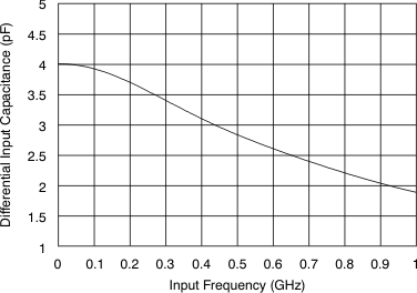 Figure 73. ADC Analog Input Capacitance (CIN) Across Frequency
9.1.2.2 Driving Circuit
Figure 74, Figure 75, and Figure 76 show examples of driving circuit configurations optimized for low bandwidth (to support low input frequencies), high bandwidth (to support higher input frequencies), and very high bandwidth, respectively. Note that each of the drive circuits has been terminated by 50 Ω near the ADC side. The transformers (such as ADTL1-1WT or WBC1-1) can be used up to 270 MHz IF. For very high IF (> 270 MHz), transformer ADTL2-18 can be used. The termination is accomplished by a 25-Ω resistor from each input to the 0.95-V common-mode (VCM) from the device. This architecture allows the analog inputs to be biased around the required common-mode voltage.
The mismatch in the transformer parasitic capacitance (between the windings) results in degraded even-order harmonic performance. Connecting two identical RF transformers back-to-back helps minimize this mismatch; good performance is obtained for high-frequency input signals. An optional termination resistor pair may be required between the two transformers, as shown in Figure 74, Figure 75, and Figure 76. The center point of this termination is connected to ground to improve the balance between the P and M sides. The values of the terminations between the transformers and on the secondary side must be chosen to obtain an effective 50 Ω (in the case of 50-Ω source impedance).
 Figure 74. Drive Circuit With Low Bandwidth (for Low Input Frequencies Less Than 150 MHz)
 Figure 75. Drive Circuit With High Bandwidth (for High Input Frequencies Greater Than 150 MHz and Less Than 270 MHz)
 Figure 76. Drive Circuit With Very High Bandwidth (Greater Than 270 MHz)
All of these examples show 1:1 transformers being used with a 50-Ω source. As explained in the Drive Circuit Requirements section, this configuration helps to present a low source impedance to absorb the sampling glitches. With a 1:4 transformer, the source impedance is 200 Ω. The higher source impedance is unable to absorb the sampling glitches effectively and can lead to degradation in performance (compared to using 1:1 transformers).
In almost all cases, either a band-pass or low-pass filter is required to obtain the desired dynamic performance, as shown in Figure 77. Such filters present low source impedance at the high frequencies corresponding to the sampling glitch and help avoid performance losses associated with the high source impedance.
 Figure 77. Drive Circuit With a 1:4 Transformer
9.1.3 Clock Input
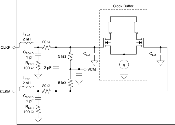
The ADS4229 clock inputs can be driven differentially (sine, LVPECL, or LVDS) or single-ended (LVCMOS), with little or no difference in performance between them. The common-mode voltage of the clock inputs is set to VCM using internal 5-kΩ resistors. This setting allows the use of transformer-coupled drive circuits for sine-wave clock or ac-coupling for LVPECL and LVDS clock sources are shown in Figure 78, Figure 79, and Figure 80. The internal clock buffer is shown in Figure 81.
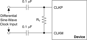
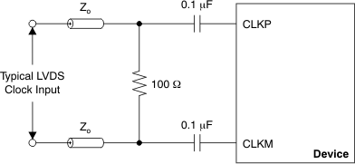 Figure 79. LVDS Clock Driving Circuit
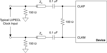 Figure 80. LVPECL Clock Driving Circuit
A single-ended CMOS clock can be ac-coupled to the CLKP input, with CLKM connected to ground with a 0.1-μF capacitor, as shown in Figure 82. For best performance, the clock inputs must be driven differentially, thereby reducing susceptibility to common-mode noise. For high input frequency sampling, it is recommended to use a clock source with very low jitter. Band-pass filtering of the clock source can help reduce the effects of jitter. There is no change in performance with a non-50% duty cycle clock input.
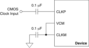 Figure 82. Single-Ended Clock Driving Circuit
9.2 Typical Application
An example schematic for a typical application of the ADS4229 is shown in Figure 83.
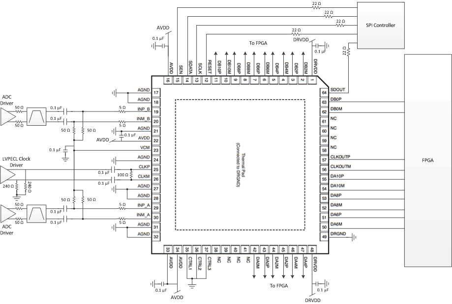 Figure 83. Example Schematic for ADS4229
9.2.1 Design Requirements
Example design requirements are listed in Table 11 for the ADC portion of the signal chain. These do not necessary reflect the requirements of an actual system, but rather demonstrate why the ADS4229 may be chosen for a system based on a set of requirements.
Table 11. Example Design Requirements for ADS4229
| DESIGN PARAMETER | EXAMPLE DESIGN REQUIREMENT | ADS4229 CAPABILITY |
|---|---|---|
| Sampling rate | ≥ 245.76 Msps to allow 80 MHz of unaliased bandwidth | Max sampling rate: 250 Msps |
| Input frequency | > 250 MHz to accommodate full 2nd nyquist zone operation | Large signal –3 dB bandwidth: 400 MHz |
| SNR | > 65 dBFS at –1 dFBS, 170 MHz | 69.8 dBFS at –1 dBFS, 170 MHz |
| SFDR | > 75 dBc at –1 dFBS, 170 MHz | 80 dBc at –1 dBFS, 170 MHz |
| Input full scale voltage | 2 Vpp | 2 Vpp |
| Channel-to-channel isolation | < 80 dB | 95 dB |
| Overload recovery time | < 3 clock cycles | 1 clock cycle |
| Digital interface | Parallel LVDS | Parallel LVDS |
| Power consumption | < 300 mW per channel | 273 mW per channel |
9.2.2 Detailed Design Procedure
9.2.2.1 Analog Input
The analog inputs of the ADS4229 are typically driven by a fully differential amplifier. The amplifier must have sufficient bandwidth for the frequencies of interest. The noise and distortion performance of the amplifier will affect the combined performance of the ADC and amplifier. The amplifier is often AC coupled to the ADC to allow both the amplifier and ADC to operate at the optimal common mode voltages. It is possible to DC couple the amplifier to the ADC if required. An alternate approach is to drive the ADC using transformers. DC coupling cannot be used with the transformer approach.
9.2.2.2 Common Mode Voltage Output (VCM)
The common mode voltage output is shared between both ADC channels. To maintain optimal isolation, an LC filter may need to be placed on the VCM node between the channels (not shown in schematic). At a minimum, a bypass capacitor should be placed on the node that has sufficiently low impedance at the desired operating frequencies. Note the VCM pin maximum output current in the electrical tables when using VCM in alternate ways.
9.2.2.3 Clock Driver
The ADS4229 supports both LVDS and CMOS interfaces. The LVDS interface should be used for best performance when operating at maximum sampling rate. The LVDS outputs can be connected directly to the FPGA without any additional components. When using CMOS outputs resistors should be placed in series with the outputs to reduce the output current spikes to limit the performance degradation. The resistors should be large enough to limit current spikes but not so large as to significantly distort the digital output waveform. An external CMOS buffer should be used when driving distances greater than a few inches to reduce ground bounce within the ADC.
9.2.2.4 Digital Interface
The ADS4229 supports both LVDS and CMOS interfaces. The LVDS interface should be used for best performance when operating at maximum sampling rate. The LVDS outputs can be connected directly to the FPGA without any additional components. When using CMOS outputs resistors should be placed in series with the outputs to reduce the output current spikes to limit the performance degradation. The resistors should be large enough to limit current spikes but not so large as to significantly distort the digital output waveform. An external CMOS buffer should be used when driving distances greater than a few inches to reduce ground bounce within the ADC.
9.2.3 Application Curve
Figure 83 shows the results of a 10-MHz LTE signal centered at 184.32 MHz captured by the ADS4229.
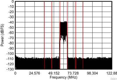
| Ref. Power = –11.98 dFBS | Lower Adj. = 69.92 dBc | Lower Alt. = 70.28 dBc |
| Upper Adj. = 69.92 dBc | Upper Alt. = 70.17 dBc |