SBOA345 June 2021 ADC10D1000QML-SP , ADC12D1600QML-SP , ADC12D1620QML-SP , INA1620 , OPA132 , OPA134 , OPA1602 , OPA1604 , OPA1611 , OPA1612 , OPA1622 , OPA1632 , OPA1637 , OPA1641 , OPA1642 , OPA1644 , OPA1652 , OPA1654 , OPA1655 , OPA1656 , OPA1662 , OPA1664 , OPA1671 , OPA1677 , OPA1678 , OPA1679 , OPA1688 , OPA1692 , OPA2132 , OPA2134 , OPA4132 , OPA4134
All trademarks are the property of their respective owners.
Resistors can be a major contribution to the overall noise of an audio circuit. The noise generated from a resistor, also known as thermal noise, is noise generated by the random motion of charges within the resistor. We can calculate the noise generated by an ideal resistor using Equation 1.
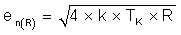
Where
Figure 1-1 displays the relationship between noise spectral density (in nV/√Hz) and resistance (in ohms) plotted for T = 25°C (298K) with varying source resistance values. At just 1k ohms of source resistance the voltage noise is already at 4nV/√Hz.
It’s important to note that an ideal resistor will exhibit predictable noise density that is flat across the frequency spectrum. Multiplying Equation 1 by the noise bandwidth yields RMS. The noise bandwidth is the bandwidth of your circuit. This bandwidth can either be set by the operational amplifier internal circuitry or by using a filter. This RMS noise calculation is shown in Equation 2.
An operational amplifier has a voltage noise and current noise source. The magnitude of the noise sources inside the amplifier is given in the amplifier’s data sheet. When considering the voltage noise of an amplifier, it is important to realize the architecture of the amplifier. Typically, a bipolar input amplifier will have much lower voltage noise than a CMOS input amplifier for the same amount of quiescent current. For more information on the difference between amplifier architectures see this technical article: Trade-offs Between CMOS, JFET, and Bipolar Input Stage Technology. Before discussing the different types of voltage noise, it’s important to understand what this noise looks like in an amplifier circuit. Amplifier noise can be simplified by modeling it as an external voltage noise en(v) on the positive terminal of the amplifier as shown in Figure 2-1.
Amplifier voltage noise can be broken down into two main components: flicker noise and broadband noise. Figure 1-1 displays these noise regions.
Flicker noise, or 1/f noise, is considered to be in the low frequency range; that is, frequencies less than 1kHz. 1/f noise has a slope of one divided by the square root of frequency. For low-frequency focused circuits, such as a woofer or bass control stage, 1/f noise can be critical. However for a circuit that covers the full audio bandwidth, the 1/f noise will not be a dominant noise contribution.
Broadband noise, also called wide-band noise, is considered to be in the middle-to-high frequency range; for example, frequencies greater than 1kHz. In most amplifier data sheets, this noise spectral density specification is shown at frequencies of 1kHz and 10kHz.
As previously mentioned, amplifiers have a current noise contribution shown as IN in Figure 2-2. Current noise is represented as a noise source between the inverting and non-inverting inputs. Input current noise density (in) is most commonly shown in the amplifier data sheet in units of. For current noise calculations, it is often necessary to calculate Req, the equivalent resistance seen by the input, shown in Figure 3-1.
The parallel combination of Rf and R1 act like a resistance on the amplifier’s non-inverting input, so Req in this example has a value of approximately 1kΩ.
This Req value can be multiplied by the input current noise density specification from the amplifier’s data sheet to yield the noise contribution due to current noise, in units of V/√Hz. This calculation is shown in Equation 3.
Multiplying the spectral density by the square root of the noise bandwidth gives RMS voltage noise. This is shown in Equation 4.
Using the OPA1656 and OPA1612 we can see how the different noise sources can affect the overall noise. Using excel we can plot out the voltage noise, current noise, and resistance noise vs resistance values. For this example, the frequency is set to 1kHz.
As the source resistance increases, the overall noise of the OPA1612 will eventually dominate that of the OPA1656 due to the current noise. For this reason, it is paramount to understand the system and all its noise contributions before choosing an amplifier.
Now, we run through a hand calculation to find the total noise of a simplified audio system. For this example, we are using the OPA1656 in a non-inverting configuration with a gain of 40 dB or 100V/V. We are also using filtering as described in Section 1 to limit the BW. Figure 4-1 is the circuit configuration we are using for this example.
The first step is to calculate the noise BW of the circuit. The cutoff frequency of the circuit in the example is set at 25.9K. The bandwidth noise of our circuit can be calculated using Equation 5.
Where:
Equation 6 is the noise bandwidth for the circuit shown in Figure 4-1.
We start by looking at the thermal noise for the circuit. The thermal noise a circuit that can be calculated by first calculating the Req of the gain network. This is completed by putting R1 and R2 in parallel. For the circuit shown in Circuit 1 this is done using the following:
At higher speeds the DC blocking cap will act like a short. For this reason, the R4 resistor is considered in parallel with the source resistance. This value is very low and for that reason is not included in the Req calculation. Using Equation 1, the 2RMS voltage noise contribution from the resistors can be calculated.
Next, we look at the voltage noise of the circuit. When evaluating the voltage noise contribution from the operational amplifier, the first step is to take the input voltage noise shown in the data sheet and multiply it by the square root of the frequency. If we look at the voltage noise from the OPA1656 SoundPlus Ultra-low Noise and Distortion, Burr-Brown Audio Operational Amplifier data sheet we see that the value is 2.9 nV/rtHz at 10kHz. As we have shown in Figure 1-1 the broadband noise will remain flat across frequency, so we can use this number for any frequencies past 10KHz. Taking the voltage noise of the amplifier times our cutoff frequency will yield the RMS voltage noise of the amplifier.
The next step is to calculate the current noise contribution of the amplifier. Using Equation 4 it is possible to calculate the RMS current noise contribution of the amplifier. For this example, the current noise of the OPA1656 is 6 fA/rtHz.
This will give what is known as the total input refereed voltage noise. Next multiply the input referred voltage noise by the voltage noise gain, which for our circuit is 100V/V. Remember this is the gain at the non-inverting terminal of the amplifier.
Based on our calculations we have a value of 100uVpp. This is very close to the simulated value of the circuit shown in Figure 4-2. Note that for a more accurate calculation, the 1/f noise may be calculated separately. For more information on voltage noise and how to calculate this error, follow these training videos: TI Precision Labs - Op Amps: Noise.
One of the key reasons for doing the calculations manually, is that it allows you to evaluate the individual noise sources. In our example, we actually see that the resistor noise is our highest noise source.