SBOK075 October 2023 SN54SC245-SEP
PRODUCTION DATA
2 Single-Event Effects (SEE) Mechanisms
The primary single-event effect
(SEE) event of interest in the SN54SC245-SEP is the destructive single-event latch-up.
From a risk or impact perspective, the occurrence of an SEL is potentially the most
destructive SEE event and the biggest concern for space applications. In mixed
technologies such as the Linear BiCMOS (LBC9) process used for SN54SC245-SEP, the CMOS
circuitry introduces a potential SEL susceptibility. SEL can occur if excess current
injection caused by the passage of an energetic ion is high enough to trigger the
formation of a parasitic cross-coupled PNP and NPN bipolar structure (formed between the
p-substrate and n-well and n+ and p+ contacts). The parasitic bipolar structure
initiated by a single-event creates a high-conductance path (inducing a steady-state
current that is typically orders-of-magnitude higher than the normal operating current)
between power and ground that persists (is latched) until power is removed or until the
device is destroyed by the high-current state. The process modifications applied for
SEL-mitigation were sufficient, as the SN54SC245-SEP did not exhibit SEL with heavy-ions
up to an LETEFF of 43 MeV-cm2 / mg at a fluence of 1 ×
107 ions / cm2 and a chip temperature of 125°C.
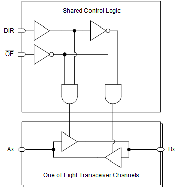
 Figure 2-1 Functional Block Diagram of
the SN54SC245-SEP
 Figure 2-1 Functional Block Diagram of
the SN54SC245-SEP