SBOU296A April 2023 – September 2023 PGA855
8.2 PCB Layout
The PGA855EVM is a four-layer PCB design. Figure 8-2 to Figure 8-6 show the PCB layer illustrations. The top layer consists of all signal path traces, and is poured with a solid ground plane. A symmetrical board layout is used at the differential inputs and outputs to keep good performance matching and improve common-mode noise rejection. Route traces as symmetrically as possible for both positive and negative pathways. The optional differential input low-pass filter capacitor is placed in very close proximity to the PGA inputs to reduce extrinsic noise. Capacitor C1 is placed in close proximity to VOCM to avoid injecting common-mode noise. Decoupling capacitors C2, C15, C3 and C16 are positioned on the top layer as close as possible to the power-supply pins of the device. The second internal layer is a dedicated solid GND plane. Independent vias are placed at the ground connection of every component to provide a low-impedance path to ground. The third internal layer and bottom layer route the input stage power supplies and the output-stage supply connections.
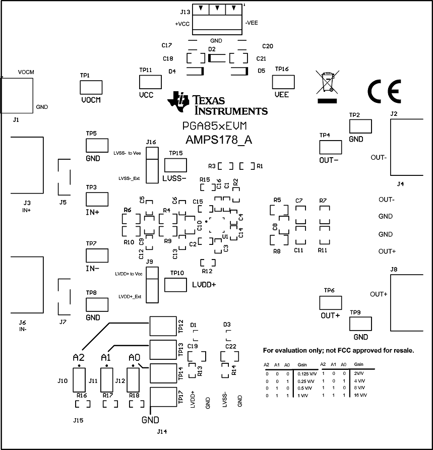 Figure 8-2 Top
Overlay PCB Layout
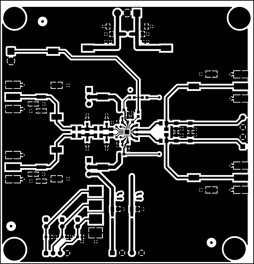 Figure 8-3 Top Layer
PCB Layout
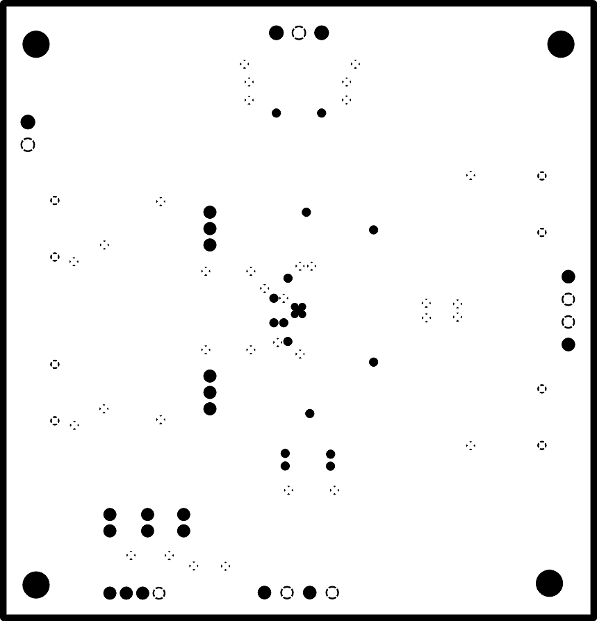 Figure 8-4 Ground
Layer PCB Layout
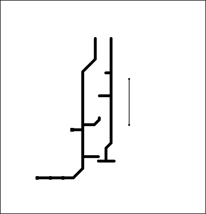 Figure 8-5 Power
Layer PCB Layout
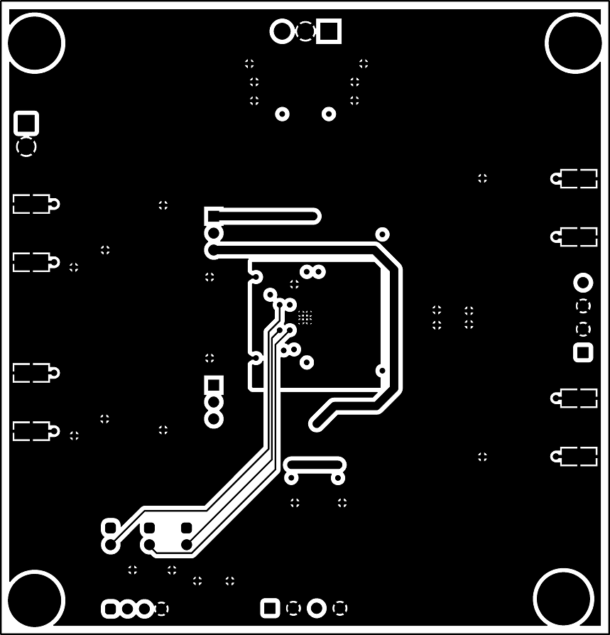 Figure 8-6 Bottom
Layer PCB Layout