SBOU296A April 2023 – September 2023 PGA855
3 Jumper Settings
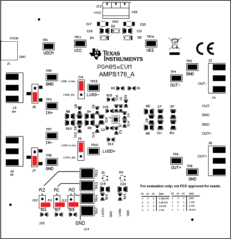
Figure 3-1 details the default jumper settings of the PGA855EVM. Table 3-1 explains the configuration for these jumpers.
 Figure 3-1 PGA855EVM Default Jumper Settings
Table 3-1 Default Jumper Configuration
| Jumper | Function | Default Position | Description |
|---|---|---|---|
| J5 | Positive (noninverting) input, IN+ | Shunt 2-3 | Shunt 2-3: Input signal to SMA connector J3 Shunt 1-2 connects IN+ to GND |
| J7 | Negative (inverting) input, IN– | Shunt 2-3 | Shunt 2-3: Input signal to SMA connector J6 Shunt 1-2 connects IN– to GND |
| J9 | LVDD+ connection | Shunt 1-2 | Shunt 1-2: Sets output stage supply LVDD+ to +VCC supply Shunt 2-3 connects LVDD+ to external connector J14 pin 1 |
| J16 | LVSS– connection | Shunt 1-2 | Shunt 1-2: Sets output stage supply LVDD- to –VEE supply Shunt 2-3 connects LVDD– to external connector J14 pin 3 |
| J10 | PGA gain CTRL A2 | Open | Open: Sets A2 to GND or 0 Shunt 1-2: Sets A2 to VCC or 1 |
| J11 | PGA gain CTRL A1 | Open | Open: Sets A1 to GND or 0 Shunt 1-2: Sets A1 to VCC or 1 |
| J12 | PGA gain CTRL A0 | Open | Open: Sets A0 to GND or 0 Shunt 1-2: Sets A0 to VCC or 1 |