SBVU068 august 2023 TPS7A78
- 1
- Description
- Features
- 4
- 1Evaluation Module Overview
-
2Hardware
- 2.1 Setup
- 2.2
Jumper Information
- 2.2.1 J1: LDO_IN
- 2.2.2 J2: Line VAC
- 2.2.3 J3: LDO_OUT
- 2.2.4 J4: LDO_IN Sense
- 2.2.5 J5: SCIN
- 2.2.6 J6: LDO_OUT Sense
- 2.2.7 J7: LDO_OUT/GND
- 2.2.8 J8: LDO_IN/GND
- 2.2.9 J9, J11, J13: GND
- 2.2.10 J10: Neutral VAC
- 2.2.11 J12: Second Surge Resistor Jumper
- 2.2.12 J14: Full-Bridge (FB) and Half-Bridge(HB) Configurations
- 2.2.13 J15: LDO Pin test header
- 2.2.14 J16 and J18: Power-Good (PG) and Power-Fail (PF) Signals
- 2.2.15 J17: Coin Cell Buffer VCC Jumper
- 2.3 Test Points
- 3Implementation Results
- 4Hardware Design Files
- 5Compliance Information
- 6Additional Information
5.1.2 Passing Pre-Compliance Conducted Emission Test Results Using Capacitors, Resistors and Inductors in the Input Filter
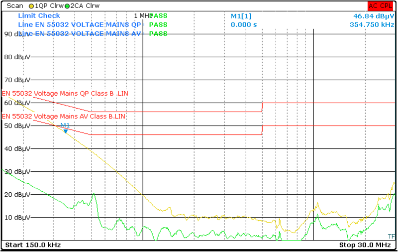
In the pre-compliance testing, the EVM has passed FCC Part 15 and CISPR 22 CLASS B CONDUCTED EMI LIMIT tests. The EVM passing the standard utilizing an introduced inductance in the loop on the R4 resistor footprint is shown below.
Section 5.1.2 curves all configured with the following: TJ = 25 °C, LDO_OUT = 3.6 V, VAC = 120 V, R4 = 100 Ω, C7 = 100 nF, R2 = 75 Ω, IOUT = 60 mA (unless otherwise noted)
 Figure 5-10 FB, Iout = 30 mA, R4 = 100
uH