SCDA008C
June 2021 – November 2021
CD4052B
,
TS3A225E
,
TS3A44159
Trademarks
1
Introduction
2
Semiconductor Switches
2.1
NMOS Switch
2.2
PMOS Switch
3
Basic Signal-Switch Structures
3.1
NMOS Series Switch
3.2
NMOS/PMOS Parallel Switch
3.3
NMOS Series Switch with the Charge Pump
4
Key Concerns in Digital-Switch Applications
4.1
Power and Control Voltage Requirements
4.2
Rail-to-Rail Operation
4.3
Undershoot
4.4
ron
4.5
Cio(off)
4.6
Cio(on)
4.7
Ci (Control Input Capacitance)
4.8
Leakage Current
4.9
Enable and Disable Delays and Propagation Delay
4.10
Partial Power Down
4.11
Voltage Translation
5
Signal Switch Families
5.1
CBT-C Family
5.1.1
Characteristics of CBT-C Family
5.1.1.1
VOvs VI
5.1.1.2
ron vs VI
5.1.1.3
Undershoot Protection
5.1.2
Application of CBT-C Family
5.1.2.1
Bus Isolation
5.2
CBTLV Family
5.2.1
Characteristics of the CBTLV Family
5.3
CB3Q Family
5.3.1
Characteristics of the CB3Q Family
5.3.1.1
VOvs VI
5.3.1.2
ron vs VI
5.3.1.3
Operation at High Frequency
5.3.1.4
Output Skew
5.3.1.5
Frequency Response
5.3.1.6
Adjacent Channel Crosstalk
5.3.2
Application of the CB3Q Family
5.3.2.1
Multiplexer in USB Applications
5.4
CB3T Family
5.4.1
Characteristics of the CB3T Family
5.4.1.1
VO vs VI
5.4.1.2
ron vs VI
5.4.1.3
Operation at High Frequency
5.4.2
Application of the CB3T Family
5.4.2.1
Voltage Translation for an External Monitor Terminal in a Notebook PC
6
Applications
6.1
Multiplexing USB Peripherals
6.2
Multiplexing Ethernet
6.3
Notebook Docking Station
7
Conclusion
8
References
9
Revision History
A Test Measurement Circuits
A.1 Measurement Setup for ron
A.2 Measurement Setup for VO vs VI Characteristics
A.3 Voltage-Time Waveform Measurement (Switch On)
A.4 Voltage-Time Waveform Measurement (Switch Off)
A.5 Output-Skew Measurement
A.6 Simulation Setup for Undershoot Measurement
A.7 Laboratory Setup for Attenuation Measurement
A.8 Laboratory Setup for Off Isolation Measurement
A.9 Laboratory Setup for Crosstalk Measurement
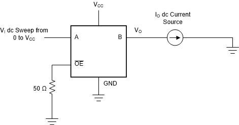
A.1
Measurement Setup for r
on
Figure 10-1
r
on
Measurement Setup