SCDA008C June 2021 – November 2021 CD4052B , TS3A225E , TS3A44159
- Trademarks
- 1Introduction
- 2Semiconductor Switches
- 3Basic Signal-Switch Structures
- 4Key Concerns in Digital-Switch Applications
- 5Signal Switch Families
- 6Applications
- 7Conclusion
- 8References
- 9Revision History
-
A Test
Measurement Circuits
- A.1 Measurement Setup for ron
- A.2 Measurement Setup for VO vs VI Characteristics
- A.3 Voltage-Time Waveform Measurement (Switch On)
- A.4 Voltage-Time Waveform Measurement (Switch Off)
- A.5 Output-Skew Measurement
- A.6 Simulation Setup for Undershoot Measurement
- A.7 Laboratory Setup for Attenuation Measurement
- A.8 Laboratory Setup for Off Isolation Measurement
- A.9 Laboratory Setup for Crosstalk Measurement
5.2.1 Characteristics of the CBTLV Family
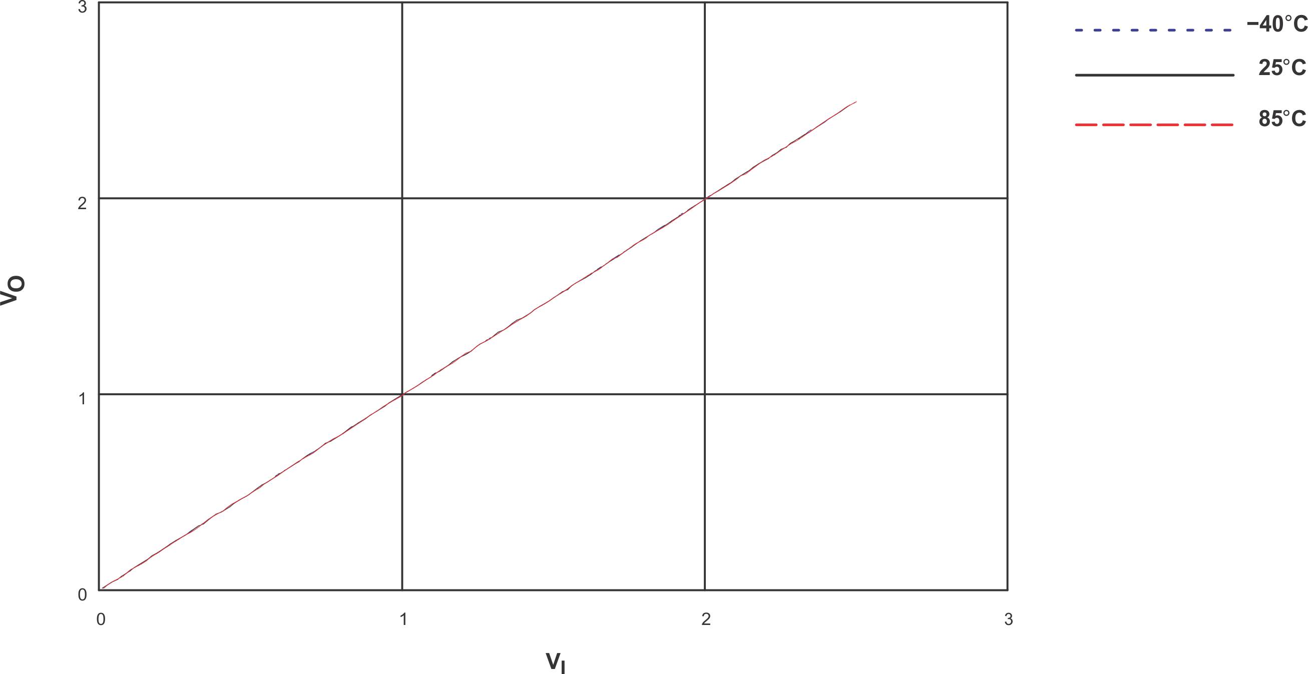
Figure 5-7 shows the VO vs. VI characteristics of the SN74CBTLV3125 and the ron flatness for VCC = 2.5 V. The output voltage exactly follows the input across the input signal range from 0 V to VCC.
 Figure 5-7 VO vs.
VI, VCC = 2.5 V (SN74CBTLV3125)
Figure 5-7 VO vs.
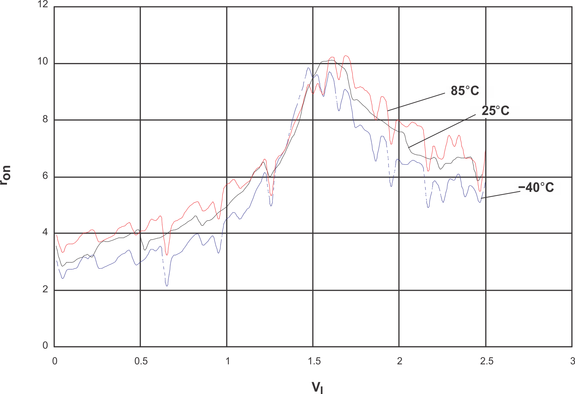
VI, VCC = 2.5 V (SN74CBTLV3125)The architecture of the CBTLV switch results in an on-resistance as low as 5 Ω. Figure 5-8 shows measurements of the on-resistance across the signal range and at different temperatures.
 Figure 5-8 ron vs.
VI, VCC = 2.5 V (SN74CBTLV3125)