SCEA112 February 2022 SN74HCS595
1 Application Brief
As electronic systems continue to shrink in size, system designers are continuously looking for smaller electronic components. Smaller components are needed to enable designers to reduce system form factors from one generation to the next without having to sacrifice system durability and ruggedness. One of the design challenges that system designers face in implementing a system’s electronic circuits is selecting integrated circuit (IC) packaging options that have both small foot prints as well as board level stability.
Historically, designers had the option of selecting larger leaded packages such as TSSOP or SOT packages, that have great board level stability resulting from the leads, or designers could choose QFN or BGA packages that provide much smaller implementation size but may not be as robust in terms of board level stability compared to a leaded package solution. In addition, electronic manufacturers that rely on optical circuit inspection, as part of their manufacturing flow, may not be able to easily incorporate QFN or BGA package technologies into their manufacturing processes.
System designers are often torn between needing the stability and the manufacturing simplicity provided by a leaded package and the smaller size of a BGA or QFN package. New packaging technologies are being developed to help system designers implement smaller more rugged system implementations.
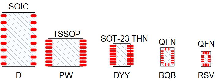
One solution that system designers can leverage today is TI’s new SOT-23-THN small leaded packaging technology. The new SOT-23-THN package is available in 5 pin (DDC), 8 pin (DDF), 14 pin (DYY) and 16 pin (DYY) pin counts. The new SOT-23-THN package is now available for a number of devices including a large assortment of logic functions. For example, the new DYY SOT-23-THN package provides one of the industry’s smallest 14 and 16 pin leaded package solutions. The DYY package is much smaller than common TSSOP packaging that designers may be familiar with (see Figure 1-1). The new DYY, DDF and DDC packages enable designers to implement solutions that take up the same or less board space than some QFN package-based devices, that perform the same function, while maintaining the 0.5mm pin pitch often needed for manageable signal routing.
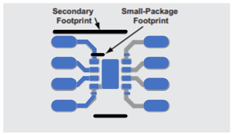
The SOT-23-THN packages provide designers with a QFN alternative for space constrained designs with the added benefits of optical inspection, easier debug, and the mechanical reliability of a leaded package. System designers who want the option to shrink new designs in the future can take advantage of the SOT-23-THN package’s ability to support dual footprint layouts with more traditional outline packages. For example, the DYY package can fit inside the traditional TSSOP footprint and can be dual routed using conventional PCB design rules.
See Figure 1-2 for example of a dual foot print layout. The new SOT-23-THN packages provide system designers yet another tool for them to leverage as they try to solve the interconnected system design challenges of shrinking form factors, board level reliability, optical circuit inspection and cost competitiveness. For more information on logic solutions available in the new SOT-23-THN packaging technology, please visit TI’s Logic and Voltage Translation.
 Figure 1-1 DYY Size Comparison with Other
Common Package Types
 Figure 1-2 DYY Package Dual Foot Print
with TSSOP Layout