SCLA069 August 2024 TPLD1201 , TPLD1201-Q1 , TPLD1202 , TPLD1202-Q1 , TPLD801 , TPLD801-Q1
Introduction
Power sequencing is a necessary application in any designs incorporating FPGAs, MCUs, or other processing units that utilize multiple power rails. Many designs require sequencing on downstream components after the components located before the downstream components, to avoid back powering or early, unintended device operation. The configurable logic and timing blocks of TPLD1201 allow for the device to provide symmetric power-up and power-down signals for numerous components. This document proposes two circuits: one which follows the structure of Figure 1, where the TPLD1201 is configured to output the maximum amount of power-up and power-down sequencing signals, and one imitating Figure 2, where external feedback verifies the TPLD1201 does not signal to power on a downstream device until the device located prior to the downstream device has been fully powered on.
 Figure 1 Power Sequencing Circuit With
Five Outputs
 Figure 2 Power Sequencing Circuit With
Feedback
Figure 2 Power Sequencing Circuit With
FeedbackDesign Considerations
- Add a decoupling capacitor between VCC and GND. Typical values are 0.1μF or 1μF. The capacitor must be placed physically close to the device.
- For better performance, the capacitive load at each output must not exceed 50pF. Verify that traces, from the device outputs, to the load switch inputs are not overtly long to avoid loading too much capacitance.
- The resistive load at the output must be greater than (VCC / IDC) Ω to verify that the absolute maximum current output ratings are not violated. This load depends on the type of output structure the output pins are programmed for (TPLD1201 pins can be programmed to be push-pull or open-drain outputs, with gains of 1X or 2X).
- If the output pins of the device are configured as open-drain NMOS or PMOS, chose the appropriate pulldown and pullup resistors of 10kΩ in ICS to avoid floating signals on the outputs.
- The voltage on the digital input pins must not exceed VCC.
- The analog input and output pins that feed into the analog comparators have a voltage range of 0-VCC V for the positive references and 0V-1.2V for the negative reference. These voltages must not be exceeded on the analog comparator pins, and care must be taken to prevent using VCC on the negative reference pin while not exceeding a maximum of 1.2V if said pin is incorporated into the design.
For this particular system, both the enable signal going into TPLD1201 and the analog feedback signals, if incorporated, must not exceed VCC of the TPLD1201. Most TI load switches draw current from the ON signal in the 10nA-30nA range and prevent overcurrent on the TPLD1201 output pins. If interfacing with an MCU or FPGA directly, care must be taken to verify that the voltage on all pins does not exceed VCC of the TPLD1201 to avoid damaging the device.
Theory of Operation
In both circuits, the input enable signal is fed into a counter block. The control data of the counter block, combined with the clock from the internal oscillator, sets the delay between each sequence signal. For example, if the oscillator is set to 25kHz (corresponding to a period of 40μs) and the counter is given a control data of 30, the delay td between the start and end of each sequence is 30μs x 40μs = 1.2ms. Since the counter reset is triggered on the rising and falling edge of the enable signal, the device does not signal to begin powering down until the input enable signal falls.
 Figure 3 Five Output Circuits in
ICS
Figure 3 Five Output Circuits in
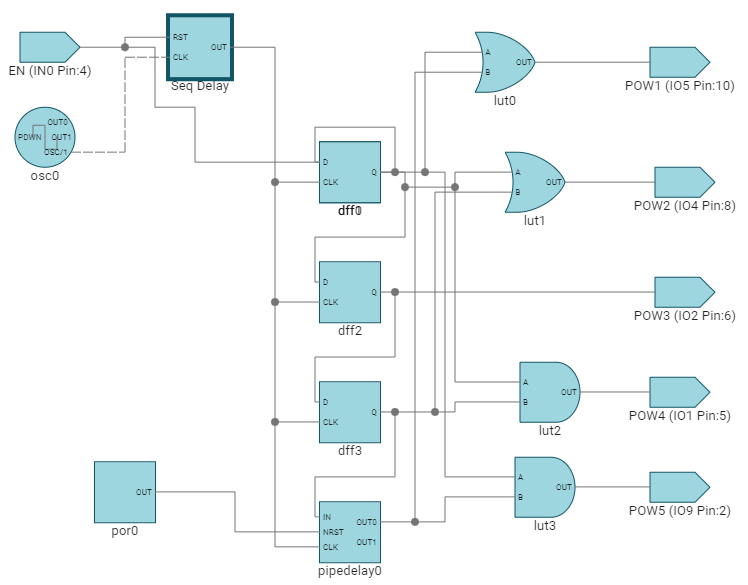
ICSIn the first circuit, whose ICS design is given in Figure 3, the counter is connected to four DFFs and a pipedelay whose OUT0 is acting as a fifth DFF. Each DFF is connected in parallel and signals power up or power down on each output when combined with the two OR and AND gates. Every additional DFF and LUT gate allows for another power sequencing output from the TPLD, with the OR and AND gates being necessary for sequential power down. Since the TPLD1201 can daisy-chain a maximum of five DFFs, up to five power sequencing signals can be sent through this design. The timing of this circuit is given in Figure 4. Each output rises and falls symmetrically around the time set by td, as described before.
 Figure 4 Five Output Circuits
Timing
Figure 4 Five Output Circuits
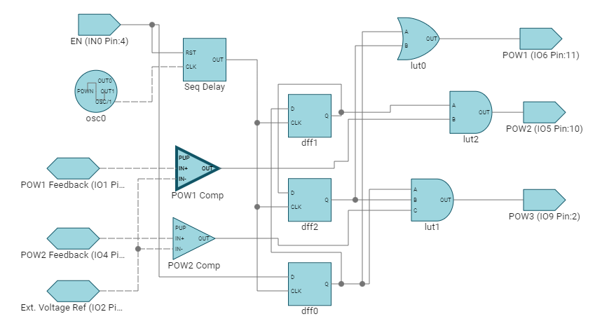
TimingAdditionally, the presence of two analog comparators allows for creating an external feedback loop that begins sequencing power to later power rails, or devices, only after the power rails located before the later power rails, or devices, have risen to a definite voltage level. The voltage level can be set up to a maximum of 1.2V, using either the internal reference voltage beginning and changing at increments of 50mV or with an external voltage reference. This application is especially useful when working with devices such as FPGAs, because the analog components are powered on before the digital I/O rails and prevent ESD or short-circuit damage. The proposed circuit is given in Figure 5 and a timing example is provided in Figure 6.
 Figure 5 Power Sequencing With Feedback
Circuit in ICS
 Figure 6 Power Sequencing With Feedback
Timing
Figure 6 Power Sequencing With Feedback
TimingConclusion
TPLD1201 is an effective design for power sequencing applications. The TPLD1201 offers a wide range of available logic and analog blocks. The I/O pins allow using the part flexibly in applications that require either a large number of sequence outputs or that require extra protection afforded by comparator feedback. The availability of these logic blocks in a single package means that TPLD1201 conserves space compared to a discrete logic option. The timing blocks of TPLD1201 allow for power sequencing implementation, without needing to include separate, appropriately sized capacitors and resistors for setting the desired RC delay for power up and power down.
References
For more details on concepts discussed in this article, refer to the following documents:
- Texas Instruments, Basics of Load Switches, application note
- Texas Instruments, Power Sequencing Reference Design Using Load Switches, design guide
- Texas Instruments, Timing of Load Switches, application note