SFFS292 October 2021 LMR54406 , LMR54410
4 Pin Failure Mode Analysis (Pin FMA)
This section provides a Failure Mode Analysis (FMA) for the pins of the LMR54410 and LMR54406. The failure modes covered in this document include the typical pin-by-pin failure scenarios:
- Pin short-circuited to Ground (see Table 4-2)
- Pin open-circuited (see Table 4-3)
- Pin short-circuited to an adjacent pin (see Table 4-4)
- Pin short-circuited to VIN (see Table 4-5)
Table 4-2 through Table 4-5 also indicate how these pin conditions can affect the device as per the failure effects classification in Table 4-1.
| Class | Failure Effects |
|---|---|
| A | Potential device damage that affects functionality |
| B | No device damage, but loss of functionality |
| C | No device damage, but performance degradation |
| D | No device damage, no impact to functionality or performance |
Following are the assumptions of use and the device configuration assumed for the pin FMA in this section:
- Device used within the 'Recommended Operating Conditions' and the 'Absolute Maximum Ratings' found in the appropriate device data sheet.
- Configuration as shown in the 'Example Application Circuit' found in the appropriate device data sheet.
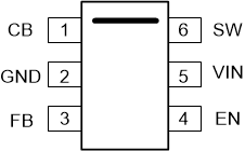
Figure 4-1 shows the LMR54410 and LMR54406 pin diagram for the SOT-23-6 package. For a detailed description of the device pins please refer to the 'Pin Configuration and Functions' section in the appropriate device data sheet.
 Figure 4-1 Pin
Diagram
Figure 4-1 Pin
Diagram| Pin Name | Pin No. | Description of Potential Failure Effect(s) | Failure Effect Class |
|---|---|---|---|
| CB | 1 | No output voltage | B |
| GND | 2 | Normal operation | D |
| FB | 3 | The regulator will operate at maximum duty cycle. Output voltage will rise to nearly the input voltage (VIN) level. Possible damage to customer load, output stage components, or both can occur. No effect on device | B |
| EN | 4 | Loss of ENABLE functionality Device will remain in shutdown mode. | B |
| VIN | 5 | Device will not operate. No output voltage will be generated. Output capacitors will discharge through input short. Large reverse current can damage the device. | A |
| SW | 6 | Damage to internal FET | A |
| Pin Name | Pin No. | Description of Potential Failure Effect(s) | Failure Effect Class |
|---|---|---|---|
| CB | 1 | No output voltage | B |
| GND | 2 | VOUT might be abnormal due to switching noise on analog circuits | B |
| FB | 3 | VOUT will be higher than the programmed output voltage. | B |
| EN | 4 | Loss of ENABLE functionality. Erratic operation; probable loss of regulation | B |
| VIN | 5 | No output voltage | B |
| SW | 6 | No output voltage | B |
| Pin Name | Pin No. | Shorted to | Description of Potential Failure Effect(s) | Failure Effect Class |
|---|---|---|---|---|
| CB | 1 | GND | No output voltage | B |
| GND | 2 | FB | The regulator will operate at maximum duty cycle. Output voltage will rise to nearly the input voltage (VIN) level. Possible damage to customer load, output stage components, or both can occur. No effect on device | B |
| FB | 3 | GND | The regulator will operate at maximum duty cycle. Output voltage will rise to nearly the input voltage (VIN) level. Possible damage to customer load, output stage components, or both can occur. No effect on device | B |
| EN | 4 | VIN | No damage to device. Loss of ENABLE functionality | B |
| VIN | 5 | SW | Damage to internal FET | A |
| SW | 6 | VIN | Damage to internal FET | A |
| Pin Name | Pin No. | Description of Potential Failure Effect(s) | Failure Effect Class |
|---|---|---|---|
| CB | 1 | No output voltage. CBOOT ESD clamp will run current to destruction. | A |
| GND | 2 | No output voltage. Damage to other pins referred to GND | A |
| FB | 3 | If VIN exceeds 16 V damage will occur. No output voltage | A |
| EN | 4 | No damage to device. Loss of ENABLE functionality | B |
| VIN | 5 | No effect | D |
| SW | 6 | Internal FET | A |