SLAU472C February 2013 – November 2023 TAS2505 , TAS2505-Q1
- 1
- Trademarks
- 1 TAS2505 Device Overview
- 2Description
-
3
TAS2505 Application
- 3.1 Terminal Descriptions
- 3.2 Audio Analog I/O
- 3.3 Analog Signals
- 3.4
Audio DAC and Audio Analog Outputs
- 3.4.1 DAC
- 3.4.2 DAC Gain Setting
- 3.4.3 Interrupts
- 3.4.4 Programming DAC Digital Filter Coefficients
- 3.4.5 Updating DAC Digital Filter Coefficients During PLAY
- 3.4.6 Digital Mixing and Routing
- 3.4.7 Analog Audio Routing
- 3.4.8 Analog Outputs
- 3.4.9 Audio Output-Stage Power Configurations
- 3.4.10 5V LDO
- 3.4.11 POR
- 3.4.12 DAC Setup
- 3.5
PowerTune
- 3.5.1 PowerTune Modes
- 3.5.2 DAC Power Consumption
- 3.5.3
Speaker output Power Consumption
- 3.5.3.1 Speaker output, Mono, 48 kHz, Highest Performance, DVDD = IOVDD = 1.8 V, AVDD = 1.8 V, SPKVDD = 3.6V
- 3.5.3.2 Speaker output, Mono, Lowest Power Consumption
- 3.5.3.3 Speaker output, Mono, 8 kHz, Highest Performance, DVDD = IOVDD = 1.8 V, AVDD = 1.8 V, SPKVDD = 3.6V
- 3.5.3.4 Speaker output, Mono, Lowest Power Consumption
- 3.5.4
Headphone output Power Consumption
- 3.5.4.1 Headphone output, Mono, 48 kHz, Highest Performance, DVDD = IOVDD = 1.8 V, AVDD = 1.8 V, SPKVDD = 3.6V
- 3.5.4.2 Headphone output, Mono, Lowest Power Consumption, DVDD = IOVDD = 1.8 V, AVDD = 1.5 V, SPKVDD = 3.6V
- 3.5.4.3 Headphone output, Mono, 8 kHz, Highest Performance, DVDD = IOVDD = 1.8 V, AVDD = 1.8 V, SPKVDD = 3.6V
- 3.5.4.4 Headphone output, Mono, Lowest Power Consumption, DVDD = IOVDD = 1.8 V, AVDD = 1.8 V, SPKVDD = 3.6V
- 3.6 CLOCK Generation and PLL
- 3.7 Digital Audio and Control Interface
- 3.8 Power Supply
- 3.9 Device Special Functions
- 4Device Initialization
-
5Example Setups
- 5.1 Example Register Setup to Play Digital Data Through DAC and Headphone/Speaker Outputs
- 5.2 Example Register Setup to Play Digital Data Through DAC and Headphone Output
- 5.3 Example Register Setup to Play AINL and AINR Through Headphone/Speaker Outputs
- 5.4 Example Register Setup to Play AINL and AINR Through Headphone Output
- 5.5 Example Register Setup to Play Digital Data Through DAC and Headphone/Speaker Outputs With 3 Programmable Biquads
- 5.6 Example Register Setup to Play Digital Data Through DAC and Headphone/Speaker Outputs With 6 Programmable Biquads
-
6Register Map
- 6.1
TAS2505 Register Map
- 6.1.1 Control Registers, Page 0 (Default Page): Clock Multipliers, Dividers, Serial Interfaces, Flags, Interrupts, and GPIOs
- 6.1.2 Control Registers, Page 1: DAC Routing, Power-Controls and MISC Logic Related Programmabilities
- 6.1.3 Page 2 - 43: Reserved Register
- 6.1.4 Page 44: DAC Programmable Coefficients RAM
- 6.1.5 Page 45 - 52: DAC Programmable Coefficients RAM
- 6.1.6 Page 53 - 61: Reserved Register
- 6.1.7 Page 62 - 70: DAC Programmable Coefficients RAM
- 6.1.8 Pages 71 – 255: Reserved Register
- 6.1.9 DAC Coefficients A+B
- 6.1.10 DAC Defaults
- 6.1
TAS2505 Register Map
- 7Revision History
6.1 TAS2505 Register Map
All features on this device are addressed using the I2C bus or SPI. All of the writable registers can be read back. However, some registers contain status information or data, and are available for reading only.
The TAS2505 contains several pages of 8-bit registers, and each page can contain up to 128 registers. The register pages are divided up based on functional blocks for this device. Page 0 is the default home page after RST. Page control is done by writing a new page value into register 0 of the current page.
The control registers for the TAS2505 are described in detail as follows. All registers are 8 bits in width, with D7 referring to the most-significant bit of each register, and D0 referring to the least-significant bit.
Pages 0, 1, 44-52 and 62-70 are available for use; however, all other pages and registers are reserved. Do not read from or write to reserved pages and registers. Also, do not write other than the Reset Values for the reserved bits and read-only bits of non-reserved registers; otherwise, device functionality failure can occur.
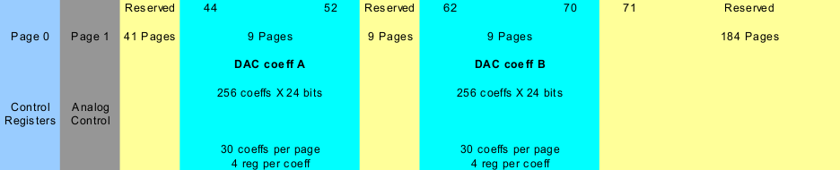
| Page Number | Description |
|---|---|
| 0 | Control Registers, Page 0 (Default Page): Clock Multipliers, Dividers, Serial Interfaces, Flags, Interrupts, and GPIOs. See Section 6.1.1. |
| 1 | Control Registers, Page 1: DAC Routing, Power-Controls and MISC Logic Related Programmabilities. See Section 6.1.2. |
| 8 - 43 | Page 8 - 43: Reserved Registers |
| 44 | Page 44: DAC Programmable Coefficients RAM. See Section 6.1.4 and Section 6.1.9. |
| 45 - 52 | Page 45 - 52: DAC Programmable Coefficients RAM. See Section 6.1.5 and Section 6.1.9. |
| 53 - 61 | Page 53 - 61: Reserved Registers |
| 62 - 70 | Page 62 - 70: DAC Programmable Coefficients RAM. See Section 6.1.7 and Section 6.1.9. |
| 71 - 255 | Page 71 -255: Reserved Registers |