SLAU863 October 2021 ADC12DJ4000RF , ADC12DJ5200RF , TRF1208
- Trademarks
- 1Features
- 2Equipment
-
3Setup Procedure
- 3.1 Install the High Speed Data Converter (HSDC) Pro Software
- 3.2 Install the Configuration GUI Software
- 3.3 Connect the EVM and TSW14J57EVM
- 3.4 Connect the Power Supplies to the Boards (Power Off)
- 3.5 Connect the Signal Generators to the EVM (Signal Generator's RF Outputs Disabled Until Directed)
- 3.6 Turn On the TSW14J57EVM Power and Connect to the PC
- 3.7 Turn On the ADCxxDJxx00RF-TRF1208-EVM Power Supplies and Connect to the PC
- 3.8 Turn On the Signal Generator RF Outputs
- 3.9 Open the ADC12DJ5200RFEVM GUI and Program the ADC and Clocks
- 3.10 Calibrate the ADC Device on the EVM
- 3.11 Open the HSDC Software and Load the FPGA Image to the TSW14J57EVM
- 3.12 Capture Data Using the HSDC Pro Software
- 4Device Configuration
- 5Troubleshooting the ADCxxDJxx00RF-TRF1208-EVM
- 6HSDC Pro Settings for Optional ADC Device Configuration
- 7Signal Routing
- 8References
- A Analog Inputs
- B Jumpers and LEDs
3.9 Open the ADC12DJ5200RFEVM GUI and Program the ADC and Clocks
The Device Configuration GUI is installed separately from the HSDC Pro installation and is a stand-alone GUI.
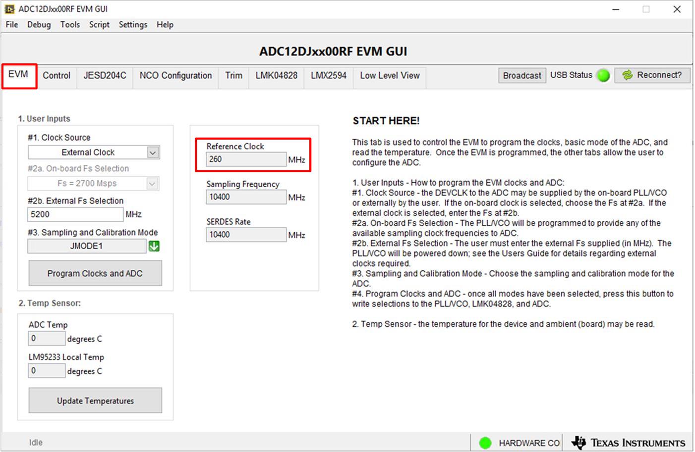
 Figure 3-2 Configuration GUI EVM Tab
Figure 3-2 and Figure 3-3 show the GUI open to the EVM tab and Control tab respectively. Tabs at the top of the panel organize the configuration into device and EVM features with user-friendly controls and a low-level tab for directly configuring the registers. The EVM has three configurable devices, namely the ADC12DJ5200RF, LMK04828, LMK61E2, and LMX2594. The register map for each device is provided in the device data sheet (ADC12DJ5200RF 10.4-GSPS Single Channel or 5.2-GSPS Dual Channel, 12-bit, RF, LMK0482xB Ultra Low-Noise JESD204B Cmplnt Clck Jitter Cleaner w/ Dual Loop PLLs, and LMX2594 15-GHz Wideband PLLatinum™ RF Synthesizer, respectively).
- Open the ADC12DJ5200RFEVM GUI.
- Select the external clock as the clock source.
- Enter Fs = 5200 MHz MSPS as the external Fs selection.
- Select JMODE1 for the sampling and Calibration mode.
- Click Program Clocks and ADC (Note: This action will overwrite any previous device register settings.)
- The Reference frequency required by the EVM is shown under indicator reference clock.