SLAU863 October 2021 ADC12DJ4000RF , ADC12DJ5200RF , TRF1208
- Trademarks
- 1Features
- 2Equipment
-
3Setup Procedure
- 3.1 Install the High Speed Data Converter (HSDC) Pro Software
- 3.2 Install the Configuration GUI Software
- 3.3 Connect the EVM and TSW14J57EVM
- 3.4 Connect the Power Supplies to the Boards (Power Off)
- 3.5 Connect the Signal Generators to the EVM (Signal Generator's RF Outputs Disabled Until Directed)
- 3.6 Turn On the TSW14J57EVM Power and Connect to the PC
- 3.7 Turn On the ADCxxDJxx00RF-TRF1208-EVM Power Supplies and Connect to the PC
- 3.8 Turn On the Signal Generator RF Outputs
- 3.9 Open the ADC12DJ5200RFEVM GUI and Program the ADC and Clocks
- 3.10 Calibrate the ADC Device on the EVM
- 3.11 Open the HSDC Software and Load the FPGA Image to the TSW14J57EVM
- 3.12 Capture Data Using the HSDC Pro Software
- 4Device Configuration
- 5Troubleshooting the ADCxxDJxx00RF-TRF1208-EVM
- 6HSDC Pro Settings for Optional ADC Device Configuration
- 7Signal Routing
- 8References
- A Analog Inputs
- B Jumpers and LEDs
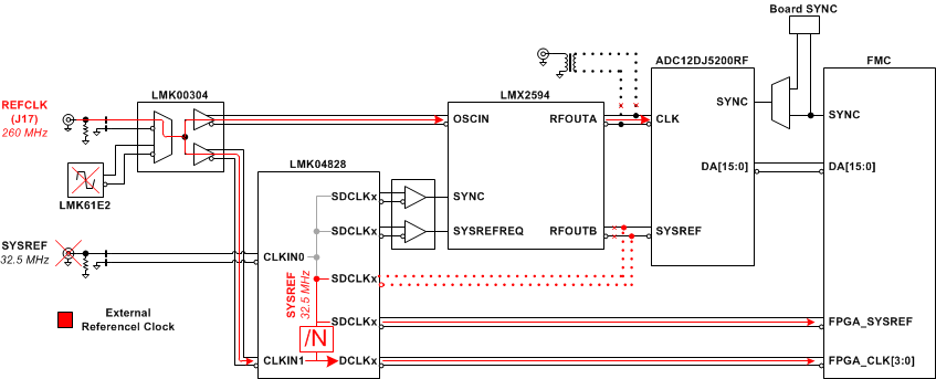
 Figure 6-3 External Reference Clocking System
Block Diagram
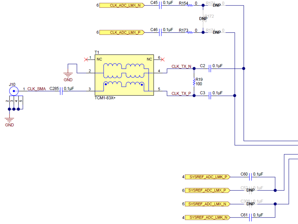
 Figure 6-4 External Clock
Configuration
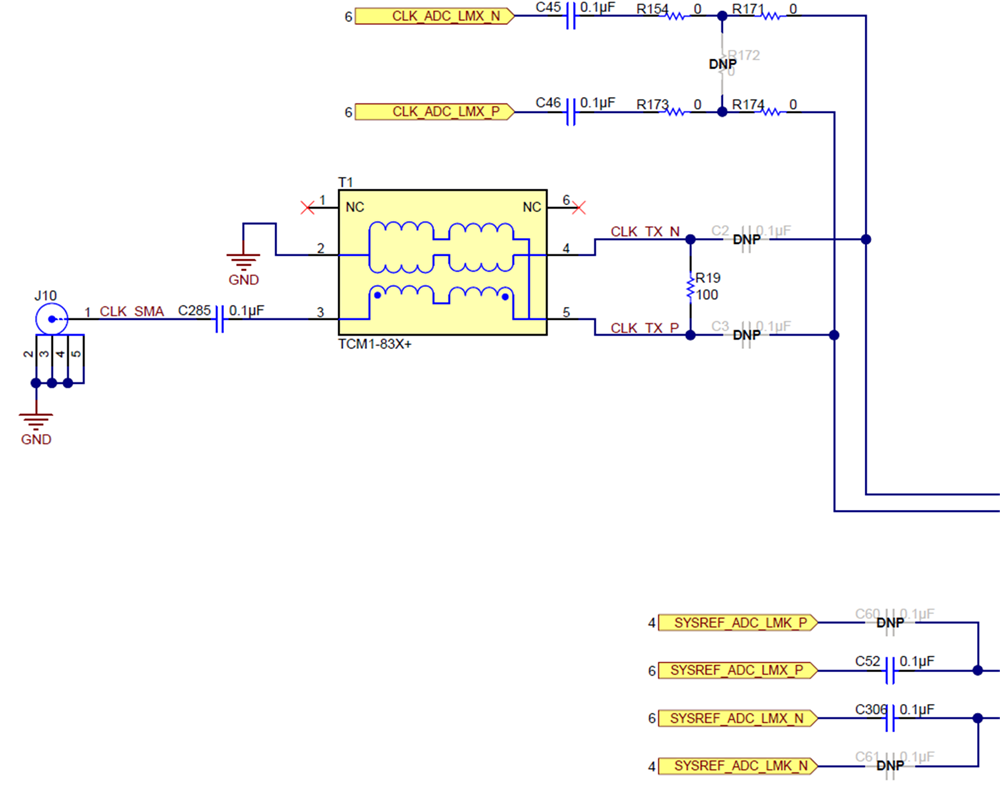
 Figure 6-5 Onboard Clocking Configuration