SLAU934 September   2024 DAC121S101-SEP


  1.   1
  2.   Description
  3.   Get Started
  4.   Features
  5.   Applications
  6.   6
  7. 1Evaluation Module Overview
    1. 1.1 Introduction
    2. 1.2 Kit Contents
    3. 1.3 Specification
    4. 1.4 Device Information
  8. 2Hardware
    1. 2.1 Hardware Setup
      1. 2.1.1 Hardware Theory of Operation
      2. 2.1.2 Jumper Definitions
      3. 2.1.3 Connector Definitions
      4. 2.1.4 Test Points
    2. 2.2 Hardware Overview
      1. 2.2.1 Electrostatic Discharge Caution
      2. 2.2.2 Connecting the FTDI Digital Controller
      3. 2.2.3 Glitch Testing
  9. 3Software
    1. 3.1 Software Setup
      1. 3.1.1 Software Installation
    2. 3.2 Software Overview
      1. 3.2.1 Launching the Software
      2. 3.2.2 Software Features
        1. 3.2.2.1 Low Level Configuration Page
        2. 3.2.2.2 High Level Configuration Page
  10. 4Hardware Design Files
    1. 4.1 Schematics
    2. 4.2 PCB Layout
    3. 4.3 Bill of Materials
  11. 5Additional Information
    1. 5.1 Trademarks
  12. 6Related Documentation

PCB Layout

The board layout for the DAC121S101SEPEVM is shown in Figure 4-3 through Figure 4-6.
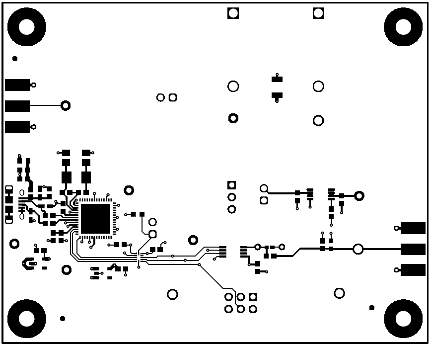
DAC121S101SEPEVM DAC121S101SEPEVM PCB Top Layer LayoutFigure 4-3 DAC121S101SEPEVM PCB Top Layer Layout
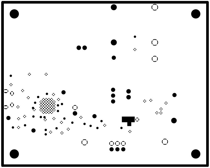
DAC121S101SEPEVM DAC121S101SEPEVM PCB Mid Layer 1 Layout (Ground Plane)Figure 4-4 DAC121S101SEPEVM PCB Mid Layer 1 Layout (Ground Plane)
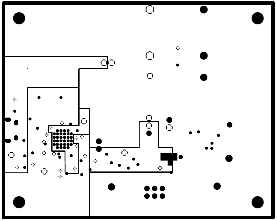
DAC121S101SEPEVM DAC121S101SEPEVM PCB Mid Layer 2 Layout (Power Plane)Figure 4-5 DAC121S101SEPEVM PCB Mid Layer 2 Layout (Power Plane)
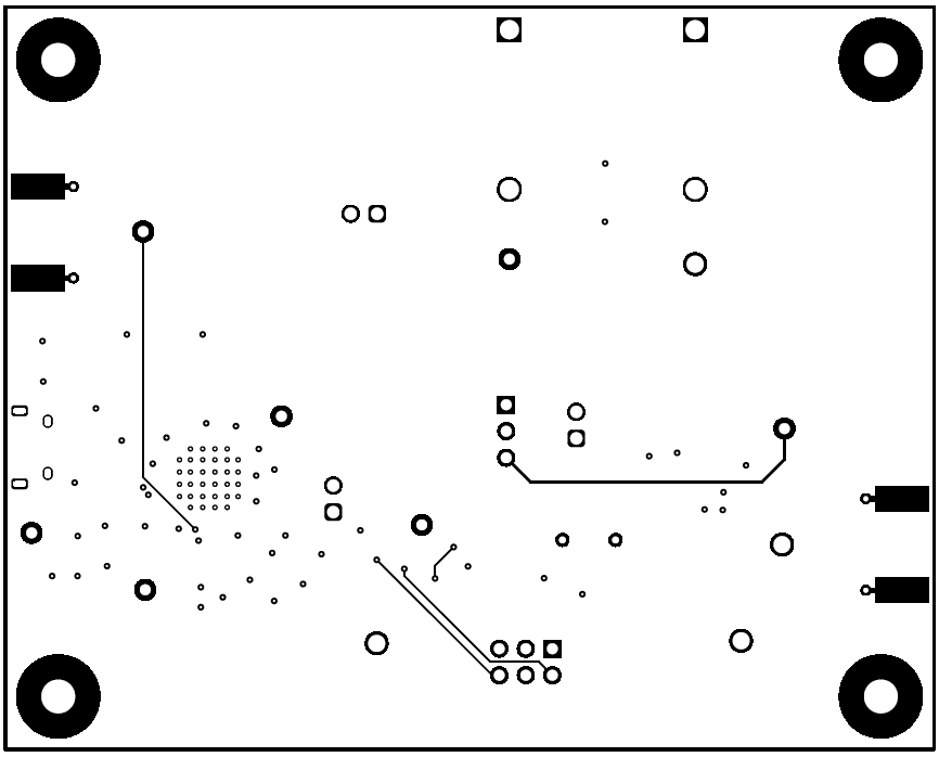
DAC121S101SEPEVM DAC121S101SEPEVM PCB Bottom Layer LayoutFigure 4-6 DAC121S101SEPEVM PCB Bottom Layer Layout