SLLA548A March 2021 – March 2022 ISO1540 , ISO1541 , ISO1640 , ISO1641 , ISO1642 , ISO1643 , ISO1644
- Trademarks
- 1 What is Isolated I2C?
- 2 What is Hot Swap?
- 3 Benefits of Hot-Swappable Isolated I2C
- 4How Hot-Swap Capability is Achieved Today
- 5Robust Communication With the Built-in Hot-Swap Feature of the ISO164x
- 6Simplified System-Level ESD Protection Design With ISO164x
- 7Conclusion
- 8References
- 9Revision History
4 How Hot-Swap Capability is Achieved Today
Today’s sensitive, high-speed serial communication devices are not all designed to support hot-swap capabilities. In isolated I2C buses where it is necessary, hot swap is typically implemented with a staggered-pin design at the point of connection, which ensures grounds and local power supplies are reliably connected before other connections are made. Figure 4-1 shows an example of a staggered male connector.
 Figure 4-1 Example of a Staggered Male
Connector Used in Hot-Swap Applications
Figure 4-1 Example of a Staggered Male
Connector Used in Hot-Swap ApplicationsSome I2C isolation devices are compatible with “power-on hot-swap” using staggered connectors or hot-swap controllers, which means I2C nodes using these devices might preserve communication on the bus only if the bus-side power supply (VCC) level of the device is always above or equal to the bus voltage levels during connection, and this is typically accomplished via hardware.
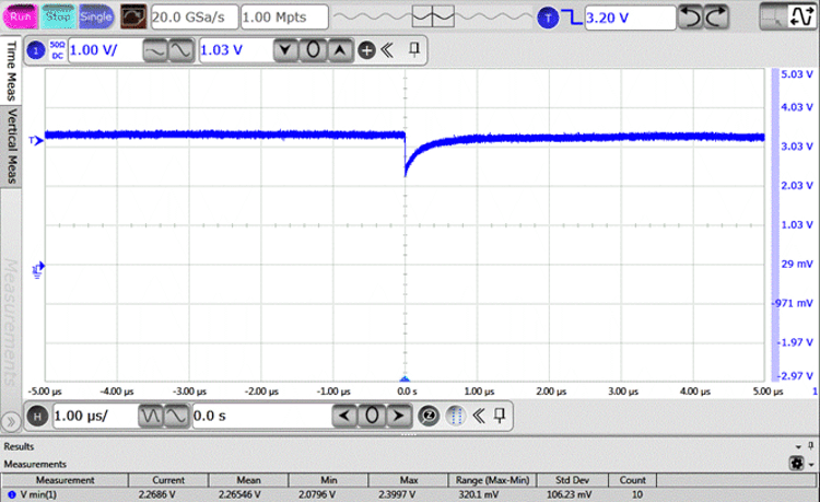
Figure 4-2 is an example of a hot-swappable isolated I2C device without pin pre-charge connected to an idle 3.3-V bus. Upon connection, plugging this partially hot-swappable device to a loaded bus reduces the bus voltage by over 60%, even in a “power-on hot swap” condition. The magnitude of this bus voltage dip varies for each system based on external factors, like the R and C values of the bus, and it could be low enough to cross the VIL, or low-level input voltage thresholds of several I2C devices, potentially causing false LOW readings by other devices connected to the bus. Compare this with an about 30% reduction when plugging ISO1640 to the same bus as shown in Figure 4-2 and Figure 4-3 .
 Figure 4-2 Regular I2C Device Without pin
Pre-charge Loading the 3.3-V bus Down to 1.2 V During Plug-in
 Figure 4-3 Pin Pre-charge in ISO1640
Reduces bus Loading to 2.3 V During a Hot-Swap Plug-in
Figure 4-3 Pin Pre-charge in ISO1640
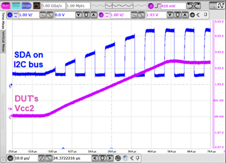
Reduces bus Loading to 2.3 V During a Hot-Swap Plug-inAs mentioned in Section 3, an I2C bus can be affected in multiple ways by devices that are not fully hot-swap-capable. Depending on the internal structure of the SDA and SCL bus pins of a device, the bus may be prevented from communicating when the device is powered down or the bus-side voltage supply, Vcc2, is ramping or left floating. Waveforms of these conditions are shown by Figure 4-4 and Figure 4-6; waveforms of the same scenario when using ISO1640 instead are shown by Figure 4-5 and Figure 4-7 .
 Figure 4-4 Regular I2C Device
Corrupting bus Communication During Plug-in
 Figure 4-5 Hot-Swappable ISO1640
Maintains Data Integrity of the bus During Plug-in
 Figure 4-6 I2C bus Clamped to
Approximately 2 V From 3.3 V by a Regular I2C Device When its
Bus-Side Power Supply is Floating
 Figure 4-7 I2C bus is
Unaffected if the Vcc2 Supply of the ISO1640 is Floating
Figure 4-7 I2C bus is
Unaffected if the Vcc2 Supply of the ISO1640 is FloatingAlong with these cases where unpowered “power-on hot swap” devices are first connected to I2C buses, similar communication errors can also occur in regular non-hot swappable devices resulting from transients coupling to unintended sections of the internal circuitry of an I2C device during every LOW-to-HIGH transition on an I2C bus if signal rise times are fast enough.