SLLA619 September 2023 ISOM8110 , TL103WB
Abstract
For battery charging applications, CC-CV charging has remained a necessary design for many products. Cost-optimized CC-CV designs are necessary to achieve sufficient charging performance without incurring significant cost. The CC-CV control loop provides analog feedback to a Switched Mode Power Supply. TL103WA is prevalent in many of these applications, as the combination of a dual op amp and integrated shunt voltage reference is both cost and space efficient, with acceptable performance. This application note uses an existing TI reference design (PMP23224), with explanations of the derivations for each of the feedback loops and some of the surrounding feedback circuitry. The CC-CV feedback loop of this reference design can be improved with two next generation components, the TL103WB and the ISOM8110. The TL103WB has improved offset, offset drift, bandwidth, quiescent current consumption, and supply voltage range over the previous generation. Additionally, leveraging TI’s new Opto-Emulators, the design can achieve improved robustness over time, performance over temperature, and increased speed of the feedback loop. This design has made some modifications to a traditional CC-CV loop. These differences are discussed and explained as well as their alternatives. The design was also created iteratively, and some trade-offs in design time can be overcome with more precise passive components, however this incurs more cost.
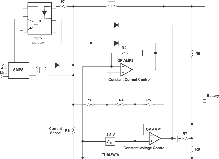 Figure 1 Typical Application
Circuit
Figure 1 Typical Application
CircuitOverview
The fundamental operation of the CC-CV charger is a high constant current operation until the battery voltage increases to a set point. Then once a certain voltage is achieved, the constant voltage control takes over to slowly charge the battery to full. In this system, the battery can be charged between 6 V to 22 V, and the maximum current delivered is 6 A. The CC-CV feedback loop uses one channel in the TL103WB as a current sense, and the other channel for voltage sense. The integrated voltage reference provides a comparison point for both error amplifiers. This application brief covers how to derive the surrounding components to complete the CC-CV feedback loop design. This is accomplished by superposition; first taking a look at the individual CC and CV loops, then combining them. Finally, showing the results of calculation and simulation. Note that the calculated and simulated values can differ slightly from each other, and can differ from a prototype. In cost-optimized designs, the best strategy is to first mathematically derive the solution, then iteratively arrive at the best component values on a prototype to achieve robust performance.
Low Battery Voltage Protection
The output voltage (Vout ) from the SMPS or flyback converter that is used for charging the battery is also used for powering the feedback amplifier and for biasing the opto-emulator. To avoid attempting to charge a battery that is too low in voltage and can be damaged from being discharged too far, a Zener diode and BJT are used as a switch to sustain a proper minimum battery voltage. Vout is connected to the collector of a BJT and to a Zener diode through a current-limiting resistor. The Zener diode is connected to the base of the transistor and establishes a maximum base voltage of 5.6 V. When the battery is 6 V or above, sufficient collector-emitter voltage is established and the proper output voltage of roughly 5 V can be seen at the emitter of the BJT. This constant 5 V feeds the amplifier feedback circuit and the isolated feedback. Keeping this voltage constant using the Zener/BJT combination allows minimization of PSRR errors and other supply-related errors on the amplifiers in the feedback loops.
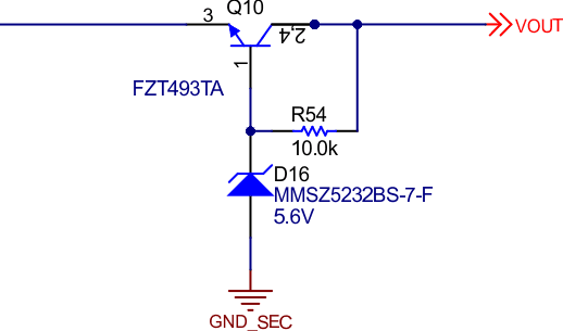 Figure 2 Battery Undervoltage
Protection Circuit
Figure 2 Battery Undervoltage
Protection CircuitShunt Voltage Reference
The TL103WB integrated shunt voltage provides a fixed 2.5-V voltage on the non-inverting input of amplifier channel one when a minimum cathode current of 1 mA is met. The maximum value of the supply resistor (R56) is constrained by the minimum cathode current, and can be calculated with Equation 1.
Maximum Supply Resistor Value:
The maximum supply resistor value is 2.5 kΩ. To allow extra current to supply enough current to properly bias the CC voltage divider and provide some overhead, a smaller value must be chosen. Therefore, a standard 1 kΩ is chosen as the supply resistor to allow 1.5 mA of cathode current margin. This margin verifies operation over passive component variation, and allows other voltage dividers to be supplied from the shunt reference.
CV Loop
Fundamentally, the CV loop is designed to feed back the Vout from the flyback converter to regulate a maximum voltage. In this circuit, a simple voltage divider feedback is used along with a classic Type 3 Compensator. More details and a full explanation of the Type 3 Compensation loop can be found in Demystifying Type II and Type III Compensators Using OpAmp and OTA for DC/DC Converters.
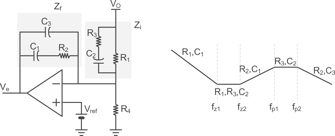 Figure 3 Type III Compensator with Gain
Curve
Figure 3 Type III Compensator with Gain
CurveIn this application brief, the method to determine the locations of the poles and zeros is covered, but not fully derived. The derivations can be found in Demystifying Type II and Type III Compensators Using OpAmp and OTA for DC/DC Converters. The component designators for setting the poles and zeros of the Type III Compensator are referenced from Figure 3. This compensator maintains the feedback loop stability. This compensator adds phase lead to the circuit and matches the classical implementation in the previously mentioned article, with one modification. Omitting the C3 from the circuit removes the highest frequency pole in the system, but the natural gain bandwidth (GBW) limitation of the TL103WB provides the final pole in the gain curve. The trade-off for this practice is a less precise setting of the final pole, and is not a recommended practice if the placement of the final pole must be precise. In this application, a precise final pole is not required. Simulation shows that even substantial movement of this final pole does not greatly change the amount of phase lead added (Figure 5), which is the main goal of the Type 3 Compensator. For a 1-MHz device, even in the excessive case of +/-600 kHz of GBW variation, the shape of the gain curve is maintained (Figure 4), and the amount of phase lead added is not changed significantly. Some decrease in phase lead can be seen at the lower end of the bandwidth variation. The new TL103WB has an increased typical bandwidth of 1.2 MHz, and variation centered around this UGBW impacts phase lead even less than the previous generation TL103WA.
 Figure 4 SPICE Simulation of Type 3
Compensator Across Bandwidth Variation
 Figure 5 Phase Lead Over Variation in
GBW
Figure 5 Phase Lead Over Variation in
GBWWithout isolation, the typical Type III Compensator bandwidth is set at 1/10th of the switching frequency of your DC/DC converter (for more information, see Switch-Mode Power Converter Compensation Made Easy). In the CC/CV circuit, which requires isolation, the dominating limit is the bandwidth of the opto-coupler. This varies with load resistance, and in this case the load resistor is 20 kΩ, which puts the -3-dB bandwidth at about 1 kHz for a traditional opto-coupler. With the new ISOM8110, the bandwidth is greatly increased, and can be set further out, allowing for a faster feedback loop.
The ESR of the electrolytic capacitors on the output of the flyback converter gives a pole on the output. The first two zeros for this loop are set to the same frequency as the complex conjugate pole. For example, a low-ESR electrolytic cap, a 470-uF cap with a 48-mOhm ESR creates a zero at about 7 kHz. Therefore, the first two zeros are set at 7 kHz. The last pole is typically set at ½ switching frequency. In the case of the TL103WB, the UGBW conveniently sets the final pole, eliminating the need for C3.
Once the locations of the poles and zeros are decided, the values of R1-R3 and C1-C3 are set using the equations in section four of Demystifying Type II and Type III Compensators Using OpAmp and OTA for DC/DC Converters. Finally, the comparison point between the two inputs is set. The Type III Compensator is going to integrate the difference between the two inputs. Thus, the Vout limit to the battery must be divided down to be equal to the 2.5-V reference voltage on the non-inverting input of amplifier one. The value of R4 is set after R1 is decided to determine the necessary voltage divider for the internal shunt reference of the TL103WB. In this case, our voltage limit is set at 22 V, and our internal reference is 2.5 V. From the standard voltage divider formula, R1 is 7.8 times larger than R4. This establishes the proper voltage limit of 22 V.
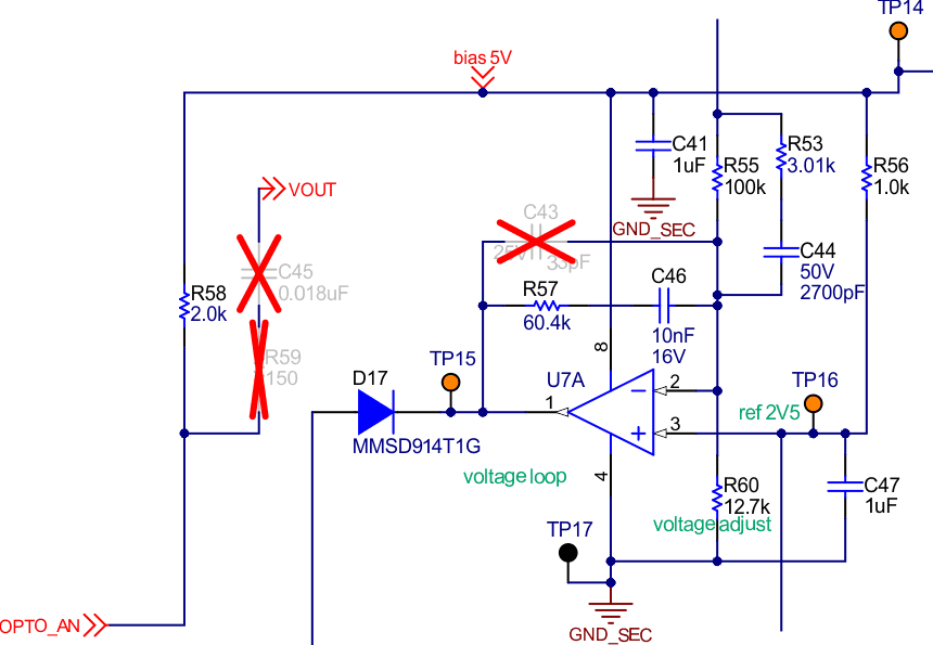 Figure 6 Full CV Loop
The error for this loop is the root sum square of the following uncorrelated errors: the tolerance of resistors R55 and R60 which form your voltage divider, the tolerance of your 2.5-V voltage reference, and the offset of your amplifier. Note that offset error has multiple factors, and for a comprehensive analysis of what goes into voltage offset, please see the TI Precision Labs Video Amplifier Offset Voltage. The TL103WB provides better voltage reference accuracy than the TL103W, and a lower offset voltage than both the TL103W and TL103WA.
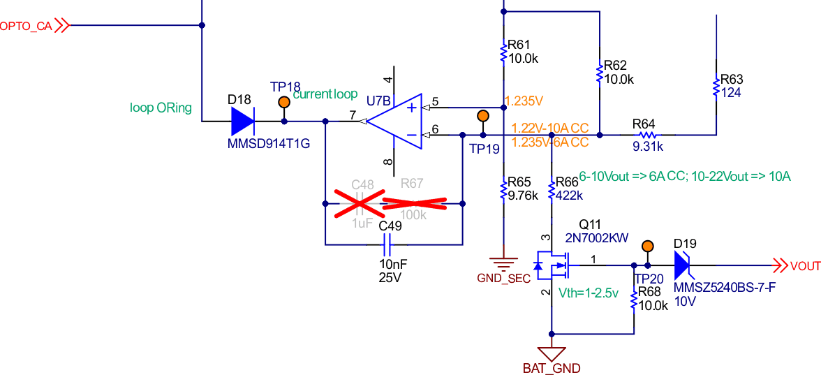 Figure 7 CC Loop Schematic
CC Loop
As seen in Figure 7, the CC loop utilizes two shunt resistors in parallel to create an equivalent 5 mΩ shunt between the battery ground and the board ground, creating a low-side current sense. This design uses standard values to create a lower equivalent resistor to minimize power loss from sensing. R61 and R65 divide the 2.5 V reference voltage to create the comparison set point for the current feedback error amplifier. R62 and R64/63 set the other side of the error amplifier. Picking standard values, Pin 5 of the TL103W is set to be 1.2348 V from the 2.5 V reference. We must also size the resistor divider to be large enough to maintain the minimum cathode current on the integrated shunt voltage reference. From the previous calculations, we have roughly 1.5 mA of current before the minimum cathode current can no longer be maintained. Since our voltage drop across both resistor dividers is roughly 2.5 V, selecting resistors with a value around 10 kΩ maintains sufficient overhead in our design. Choosing 10 kΩ and 9.76 kΩ, with a reference voltage of 2.5 V, Pin 5 is set to 1.2348 V. The other input to the error amplifier can be confusing when thought of as a voltage divider, but is better understood if thought about as an inverting summer circuit, where the common mode is held at 1.2348 V and the two resistances R62 and R64/R63 provide the weighted sums of currents into the node. In DC analysis, the amplifier does not provide current into the summing node, as C49 blocks DC current. The contribution of current each node provides aligns with Equation 3.
IIN-x is the contribution of current into or out of the node for any number of inputs with an input resistor. Applying this to our circuit, you can see that the current contribution from Vref is:
This current can be used to back-solve the R for the shunt resistor node, since we want an equal but opposite current contribution from the shunt resistor. Rearranging Equation 5 yields the following equation:
Vin x is the voltage provided from our shunt resistor. A max current of 6 A with a 5-mΩ shunt resistor gives 30 mV. Plugging this value into Equation 4, the resistance is:
The resistance between the shunt and the summing node of the amplifier is inversely proportional to the current limit. As R64/R63 decreases, the current limit set point increases. This factor is important when iterating the design. Additionally, some current limit headroom is allowed to control for offset errors and errors with passive devices around the amplifier. Using the original TL103WA, the percent error from the offset was ±5 mV which means there is ±16% error from offset voltage alone. To maintain a maximum current of 6 A, set current limit must be decreased. Centering the current limit at 4.8A, we give ample headroom to the design to account for offset at room and offset drift. The newer TL103WB can achieve a more accurate design with a simple BOM change. With a maximum offset over temperature of 2.5 mV, the offset error yields only +/-8% error. The current limit can now be centered at 5.4 A, which provides us ample headroom for the 6 A maximum current limit, without sacrificing power loss through the shunt resistor. Using this new current limit, Rx can be solved for:
To compensate this loop, there is the option to add C48 and R67 to implement a Type II Compensator circuit, the methodology for setting these poles and zeros can be found in compensation made easy. This application brief uses a zener diode and an external FET to set multiple levels of charge current once a threshold voltage has been met. In this case, once Vout reaches 10 V, a 422 k resistor is paralleled with the R64/R63 resistances to create a new set point for the current. This follows the same design methodology as above, but when calculating the resistance value, the parallel combination of resistors must be used.
Isolated Feedback
In the original design, an optocoupler was used to give an isolated feedback to the flyback converter. This design can be improved using TI’s new Opto-emulators. These opto-emulators leverage TI’s Silicon Dioxide (SiO2) technology to achieve isolation, and have several key improvements over the traditional optocouplers. Since these devices have no LED and emulate the diode instead, there are no LED aging effects, leading to a much more stable performance over time. In addition to the improved performance over time, these devices offer many other improvements. Opto-emulators exhibit flat CTR over temperature, maintaining consistent output regulation in changing environments. There is a reduced part-to-part variation, enabling improved designs with optimized efficiency. Opto-emulators have wide bandwidth which improves load transient response. System cost is reduced by reducing the requirements of the output capacitor, and barrier lifetime is improved with SiO2 insulation. In many cases, the opto-emulators can provide benefits as a drop-in replacement. To learn more about the advantages of opto-emulators read Introduction to Opto-emulators.
 Figure 8 Traditional Optical
Isolation
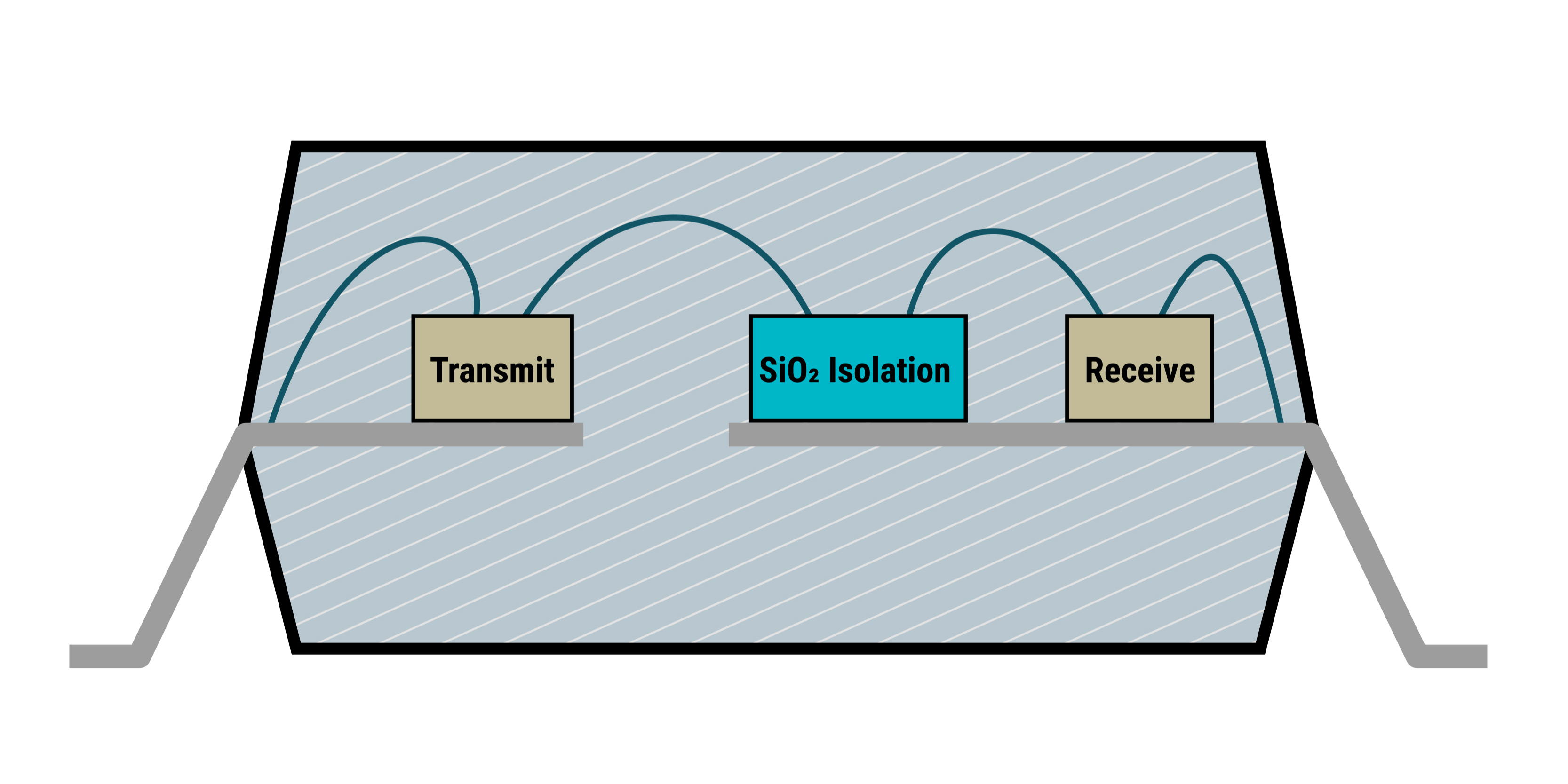 Figure 9 Opto-emulator
Isolation