SLLA623 September 2023 THVD8000 , THVD8010
4 Guidelines for a Combined System
With an understanding of the basic differences between Classical RS-485 and Powerbus it has been shown that the device cannot communicate with one another, but will not directly harm one another if communication does occur between devices. However, this presents a unique issue for designers of large networks of communication nodes in factory and/or building automation use cases where the designer may not have full control over every node in the system, but Powerbus would help significantly reduce system overall cost due to halving cabling costs. Traditionally this means the designer would implement Powerbus on internal projects where they had full control over the network and implement Classical RS-485 otherwise while having to suggest a more expensive solution to the customer until the designers of the other nodes decided to move towards Powerbus for the significantly cheaper implementation – if they do at all. This creates a situation where multiple boards will need to be designed to fit multiple niches and upgrading a system from Classical RS-485 to Powerbus would require a completely new board design. However, there is a quicker approach – a dual use board that can be configured to work as Powerbus or Classical RS-485. The remainder of this note will cover the original design parameters, schematic design, and finally a proposed layout of what a universal board could look like and the benefits and trade-offs of pursuing this type of application.
Powerbus is very flexible in its design. To be able to show an illustrative example the parameters of the design were fixed to the following requirements.
| Parameter | Requirement |
|---|---|
| Main Power Rail | 36 V DC |
| Max Current from Power Rail | 3 A |
| Total Number of Power Nodes | 4 |
| Device VCC | 5 V or 3.3 V |
| Modulation Frequency | 5 MHz |
Using the equations from section 1 it yields us the following results. The minimum series capacitance is 6.4nF – so any capacitance 6.4nF or larger should work, so for this design 1uF capacitors will be chosen. To avoid too much derating due to voltage 50V to 100V ceramic capacitors should be chosen – in general the max voltage across capacitor multiplied by 2 is a good voltage rating to have to avoid derating on ceramic capacitors. One thing to note is that capacitors of 255nF or larger can work in any Powerbus application regardless of modulation frequency in DC systems - in AC systems the capacitance value matters much more as the AC signal will conduct through the series capacitor. The minimum effective inductance per node (since there are 4 nodes – there will need to be 8 inductors) will be 48.5uH of effective inductance per power node connection. It is important to consider the saturation current of the inductor – as depending on inductor manufacturer the saturation current is the current needed to decrease inductance by either 10%, 20%, or 30% of nominal value – so while the power supply current doesn’t matter to the Powerbus device – it will matter to the inductor portion of the coupling network. With the Powerbus parameters discussed the joint schematic design can now be analyzed.
Classical RS-485 system design is much more simplistic that Powerbus – so this joint schematic would work for any device in an 8-Pin SOIC package – which is the most common package for Half-Duplex RS-485 transceivers. The Combined design can be thought of in three distinct parts: the power connections, single ended I/O, and the direct transceiver interface.
 Figure 4-1 Generalized Power Input Schematic
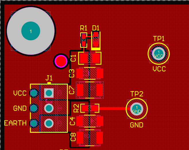
The power connections comprise themselves of two terminal block/test point inputs for the device VCC and in case of Powerbus the main power line that will comprise half of the signals on the shared bus. They are both constructed in the same way – a simple three prong input (Live, Neutral/GND, and Earth/Chassis Connection) with J1 for device VCC and J2 for the higher power signal. They both contain bulk capacitance between positive and negative terminals of source with the additional option of having additional capacitance between negative terminal of power supply and an EARTH/Chassis connection. The bulk capacitance is not necessary for the device VCC, but bulk capacitance is assumed to exist on the power source and loads by the Powerbus devices. The values of capacitance can change depending on exact use case. There is also the option included with a resistor from GND to EARTH to reduce ground loop current and therefore decreasing risk of noise issues. Beyond the power inputs there is also two more features, an LED indication light for device VCC and a shunt between GND and EARTH if an Earth connection is not present in the system. Depending on exact use case is what determines connections.
| Component | Classical RS-485 | Powerbus | Comment |
|---|---|---|---|
| J1 | Device VCC Input | Device VCC Input | Accepts 3.3V to 5V |
| TP1 | Device VCC Input + Terminal | Device VCC Input + Terminal | Same between use cases |
| TP2 | Device GND Input | Device GND Input | Same between use cases |
| J2 | Not Used | Power Line Input | Only used in Powerbus |
| TP3 | Not Used | Power Line “Live” Input | - |
| TP4 | Not Used | Power Line “Neutral” Input | - |
 Figure 4-2 Generalized Single Ended I/O Schematic
After the power connections, the next concern is single ended I/O. Luckily as discussed previously the D and R pins function identically between Classic RS-485 and Powerbus. In the most use case R and D can be directly connected to the controller of the wired communication subsystem – however loading, pull-ups and pull-down resistors can be implemented. The “R” pin above, attached to J3, has options for a pull-up, pull-down, and / or capacitive load – where a common use case would be to have a pull-up resistor and a capacitive load so an Idle state is always read as “high”- this is very common with the UART protocol. The D pin, attached to J8, shows an option of a pull-up resistor to ensure a guaranteed level at startup. It is always best practice to have a predefined “default” state on logic inputs to prevent glitching at the output – but it doesn’t have to be a pull-up as it could also be a pull-down resistor. The two other signals a bit more involved on a combined board. First looking at the DE signal, attached to J7, it is important to note that this input is only used for Classical RS-485 subsystems as the Powerbus devices do not have a DE pin. Finally, the “MODE” input on J6 is going to change its operation based on what type of application is being used. In Powerbus applications the input at J6 will be used to switch the mode (either RX (logic low) or TX (logic high)) of the transceiver and in Classical RS-485 this input is used to turn the receiver on (logic low) or off (logic high).
| Component | Classical RS-485 | Powerbus | Comment |
|---|---|---|---|
| J3 | R Pin Single Ended Output | R Pin Single Ended Output | No difference between standards |
| R5 | Optional Pull-Up | Optional Pull-Up | No difference between standards |
| R8 | Optional Pull-Down | Optional Pull-Down | No difference between standards |
| C13 | Optional Capacitive Load | Optional Capacitive Load | No difference between standards |
| J8 | D Pin Single Ended Input | D Pin Single Ended Input | No difference between standards |
| R17 | Optional Pull-Up | Optional Pull-Up | No difference between standards |
| J7 | Driver Active High Enable (DE) Control Signal Input | Not Used | DE only exists on Classical RS-485 with Standard Enables |
| R20 | Optional Pull-Down | Not Used | DE only exists on Classical RS-485 with Standard Enables |
| J6 | Receiver Active Low Enable (/RE) Control Signal Input | Mode (Mode) Control Signal Input | /RE only controls RX; Mode controls RX and TX |
| R16 | Optional Pull-Down | Optional Pull-Down | Pull-Down can exist in both standards. |
 Figure 4-3 Classical RS-485 + Powerbus Interface Schematic
Finally, the most important aspect of the combined Classical RS-485 and Powerbus is the transceivers themselves. This can be broken down into three sections – the power connection, the single ended inputs (controller facing pins), and the differential bus facing pins.
The power pins have largely already been covered previously the only adjustment is that it is required that at least 100nF of decoupling capacitance is added close to the VCC pin of the IC – this is true for both the THVD8000/THVD8010 and most other modern RS-485 devices (older devices may suggest larger capacitors such as 1uF – but most modern devices will be at 100nF) – since the board has two distinct IC footprints two 100nF capacitors were used – one by each devices VCC.
Next the single ended signals have also been largely covered – however there is an important consideration with respect to the MODE, DE, and F_SET pins between Classical RS-485 and Powerbus. The input of the Mode signal will lead to the MODE pin of the THVD8000/THVD8010 and the /RE pin of the Classical RS-485 device. In applications where the Classical RS-485 device has DE and /RE shorted together, resistors R9 and R14 can be added to create a short between these pins. When using this in Powerbus mode the resistors R9 and R14 should be removed as DE is not present in Powerbus and there are no direct inputs onto F_SET for a Powerbus application. This leaves the F_SET pin – which is unused in Classical RS-485 systems, but would be utilized in Powerbus applications by applying a resistor to device GND -the resistor chose, R13, is at a value that will set the modulation frequency to 5MHz.
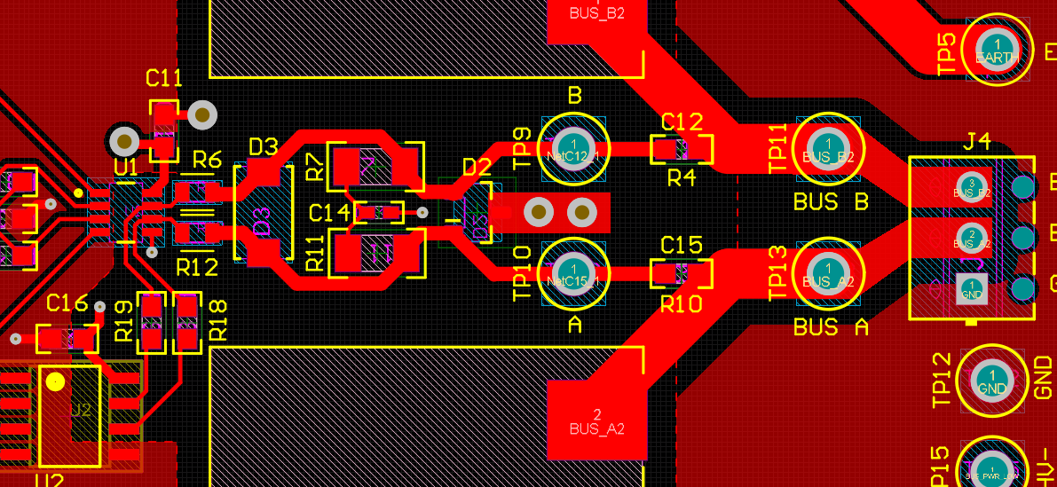
Lastly, the bus pins can be discussed. Ideally Classical RS-485 has two terminations between A and B in the system (120Ω each) with the only other circuit components being protection diodes, EMI mitigation, and/or biasing resistors; whereas Powerbus has that plus the coupling network to contend with. The first issue that may be noticed is the trouble that a Classical RS-485 transceiver will have communicating over the series capacitance; while this technically can be done it generally requires an encoding scheme that will reduce overall throughput of the system while increasing complexity of the data transmission. To get around this potential issue the board gives an option of a resistive series connection or a capacitive one. In Powerbus the capacitors would be installed while the 0Ω links would not be installed and vice versa for Classical RS-485. The next primary concern is that of the inductive coupling – technically speaking common mode inductance towards an “AC” ground reference is not expressly forbade by RS-485 standard, but minimum common mode impedance to ground is alluded to in the standard. Once again – this value is approximately 375Ω. Since the inductor’s impedance is based on frequency and there is no guarantee that the base frequency component of the unmodulated RS-485 datastream is going to maintain the correct frequency to prevent overloading on the bus without additional encoding schemes, is going to create a mismatch between overall bus loading between Classical RS-485 and Powerbus. This can be resolved by just keeping pads available for the inductors when Powerbus is needed and do not populate otherwise. The other components largely comprise of what is suggested for both Classical RS-485 and Powerbus – including a split termination, protection diodes, and a resistive link between Classical RS-485 and Powerbus connections that can be implemented when using Classical RS-485.
| Component | Classical RS-485 | Powerbus | Comment |
|---|---|---|---|
| R9 | Install if both control pins are controlled via 1 signal | Do Not Install | - |
| R14 | Install if both control pins are controlled via 1 signal | Do Not Install | - |
| R6 and R12 | Optional Pulse Proof Series Resistors | Optional Pulse Proof Series Resistors | Protects input pins during surge/transient before protection diodes begin to conduct |
| D3 | Bidirectional Protection Diode (+/-12V) | Differential TVS Protection Diode | Protects with Reference to Differential Wire |
| D2 | Dual Channel Bidirectional Protection Diode (-7V/12V) | Dual Channel Bidirectional Protection Diode (-7V/12V) | Protects with Reference to Device GND |
| R7, R11, and C14 | Split Termination – EMI mitigation; can use 120Ω resistor instead | Split Termination – EMI mitigation; can use 120Ω resistor instead | Split termination helps filter off common mode noise |
| C12 and C15 | Do Not Install | Install | Series Coupling Capacitors for Powerbus |
| R4 and R10 | Install | Do Not Install | - |
| L1 and L2 | Do Not Install | Install | - |
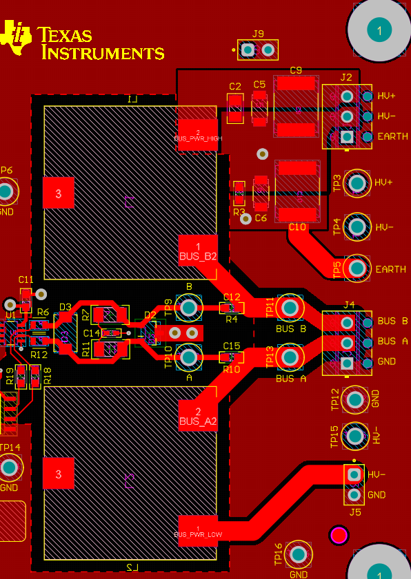
With an understanding of the schematic and how to use under which circumstances a possible layout can be constructed.
 Figure 4-4 Example Layout - Top Layer


 Figure 4-5 Close Up of Layout for IC PWR, IOs, Differential Bus, and High Power Interface
 Figure 4-6 Example Layout - Bottom Layer
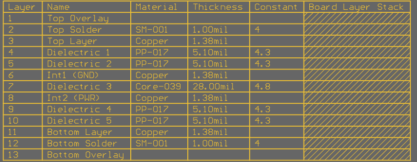
 Figure 4-7 Example Layout - Layer Stackup
The layout uses a 4-layer board to keep device VCC and GND internal to the board for ease of routing – this is not required – but can make layout easier.
With a layout and schematic, a semi-universal board is created. The benefits of which allow a single design for multiple systems. The largest tradeoff comes with solution size and Powerbus variability. Classical RS-485, due to the lack of inductors, generally will offer a smaller solution size. In space limited applications a purely Classical RS-485 approach is most likely needed. The other main tradeoff is the needs of power bus – the inductance value and size can greatly vary depending on needs of the application or end equipment – for a truly universal board inductors should be chosen at 256 nodes at 125KHz modulation with worst case power supply current considered – as this type of board will work in any power bus application at the cost of the largest solution size due to the large inductance values.