SLLA643 August   2024 MCF8315C , MCF8315C-Q1 , MCF8316C-Q1


  1.   1
  2.   Abstract
  3.   Trademarks
  4. 1Introduction
  5. 2Power Pin Design Recommendations
    1. 2.1 VM
    2. 2.2 Charge Pump: CPH, CPL, CP
    3. 2.3 Buck Converter: FB_BK, SW_BK, GND_BK
    4. 2.4 AVDD
    5. 2.5 DVDD
    6. 2.6 PGND, AGND, DGND
    7. 2.7 Thermal Pad
  6. 3MCF831xC Buck Regulator Overview
    1. 3.1 Buck Regulator Mode of Operation
    2. 3.2 Buck Regulator Output Voltage
    3. 3.3 Buck Power Sequencing
    4. 3.4 Buck Inductor Selection
    5. 3.5 MCF831xC Operation Without Buck Regulator
  7. 4MCF831xC IO Pins Design Recommendations
    1. 4.1 SPEED Pin
    2. 4.2 BRAKE, DIR, DRVOFF pins
    3. 4.3 EXT_CLK, EXT_WD
    4. 4.4 ALARM
    5. 4.5 DACOUT1, DACOUT2
    6. 4.6 SDA, SCL
    7. 4.7 nFAULT and FG pin
  8. 5MCF831xC PCB Schematic and Layout Recommendations
    1. 5.1 Single Ground Plane
    2. 5.2 Single Ground with AVDD Shorted to FB_BK
    3. 5.3 Two Grounds
  9. 6Summary
  10. 7References

Single Ground with AVDD Shorted to FB_BK

As shown in Section 4.7, for low power/cost applications where the buck regulator is disabled, the recommendation is to connect FB_BK and AVDD externally on the board. Refer to Figure 5-3 and Figure 5-4 for a sample schematic and layout for a single ground plane PCB. One additional capacitor 1uF(C7) is added close to FB_BK due to long trace from AVDD to FB_BK.
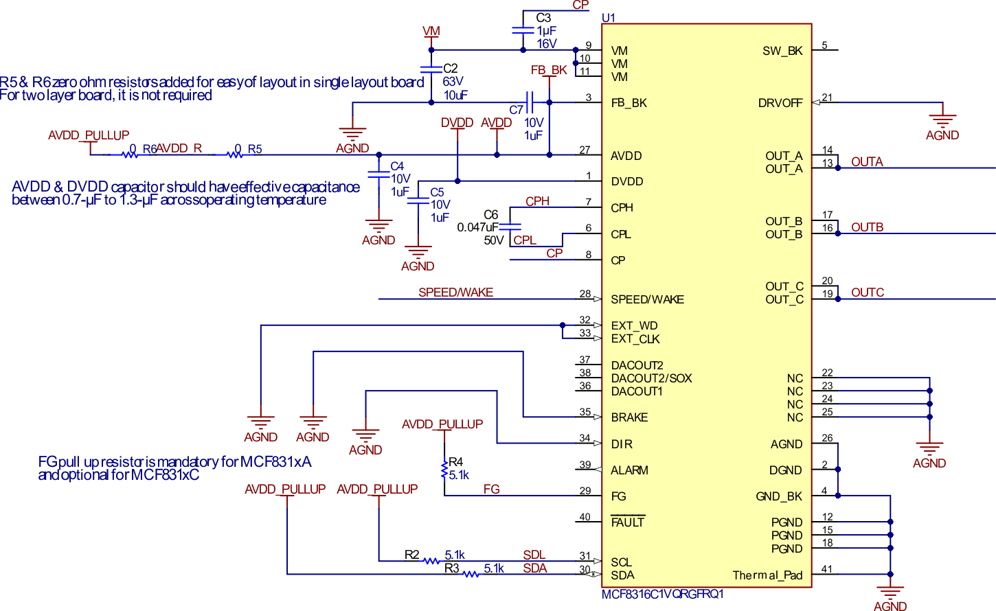
 PCB Schematic for Single
                    Ground Plane and FB_BK Powered by AVDD Figure 5-3 PCB Schematic for Single Ground Plane and FB_BK Powered by AVDD
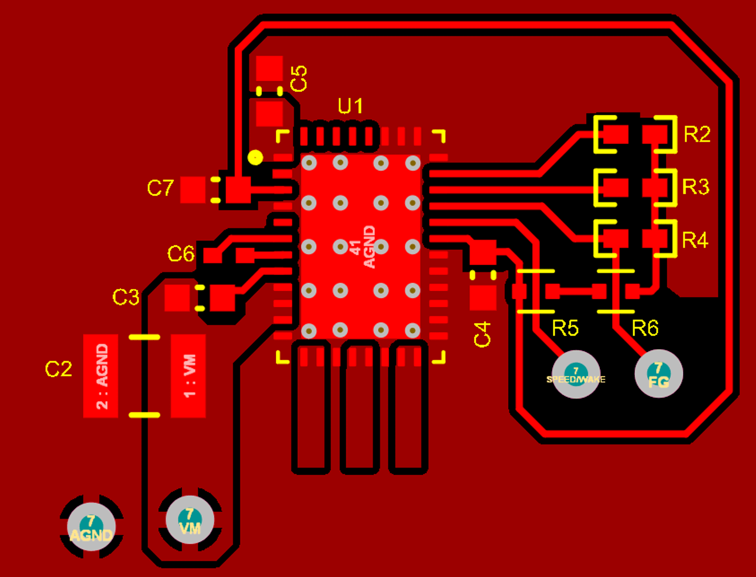
 PCB Layout for Single Ground
                    Plane and FB_BK Powered by AVDD Figure 5-4 PCB Layout for Single Ground Plane and FB_BK Powered by AVDD