SLLU365 January 2023 THVD1454
5.2 Potential Modifications
With a understanding of the board in its default state there are a few modifications that can be made either via the header blocks or by adding addition components.
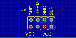
Figure 5-1 shows the control header J6, which with the addition of two shunts can control the Slew Rate Control (SLR) feature and Integrated Termination (TERM) features.
 Figure 5-1 Control Block View: J6
The J6 header has pin one on the bottom right hand corner and pin two on the top right hand corner. The pins increment up from right to left with the top row even pin numbers and the bottom row odd numbers. A signal map is shown in Table 5-4.
| J6 Pin # | SIGNAL |
|---|---|
| 1 | SLR |
| 2 | SLR |
| 3 | VCC |
| 4 | GND |
| 5 | TERM |
| 6 | TERM |
| 7 | VCC |
| 8 | GND |
A function table of SLR and TERM is shown in Table 5-5.
Pin | Jumper Pin | State | Function | Comment |
|---|---|---|---|
TERM | J6-5, J6-6 | Low | Integrated Termination Disabled | For non-terminated nodes |
TERM | J6-5, J6-6 | High | Integrated Terminatino Enabled | Terminated with 120Ω between A and B. |
SLR | J6-1, J6-2 | Low | Slew Rate Control Disabled | Max Speed is 20Mbps |
SLR | J6-1, J6-2 | High | Slew Rate Control Enabled | Max Speed is 500Kbps |
Beyond the controllable features accessed through J6 there are also pads for external pull-up, pull-down, and capacitive loads available on J1, J2, J3, and J4. For typical applications capacitive loads are placed on "R" pin and the other pins may or may not have external pull-up or pull-down resistors. All the pads are in 0603 packages and can be varied based on customers testing needs.
The final modifications are around the differential bus pins - A and B. To help simulate capacitive loading of a cable a 0805 termination capacitor pad, ID = C8, is available between A and B pins. The option to add an external termination resistance is also possible with a 0805 pad, ID = R16. This external termination when paired with the integrated termination resistor can allow for quick measurements of power measurements on a terminated bus. The power testing can be expanded with the addition of common mode loading resistances R19 and R20.