SLLU370 june 2023 THVD4431
2.2 Setup
Operational Modes and Control Signals
After the power supply of THVD4431EVM has been configured, set up the board for operation. Before any operation of the board can occur, the operational mode and control pins must be configured. In Figure 3-1, the map to the J9 header pins is shown. Assume that the board is oriented with J12 and J13 in the top left of the EVM. The numbered boxes correspond to the pin number for J9 as indicated in the schematic.
 Figure 2-1 THVD4431EVM: IC Control Header
(J9) Map
Figure 2-1 THVD4431EVM: IC Control Header
(J9) MapTo select a configuration option, find the signal of interest on J9 according to Figure 3-1. If a low value is wanted, then shunt the top row header pin connected to the signal of interest to the pin on the left. If a high is wanted shunt, then connect the bottom row header pin to the signal of interest to the pin on the left. If VIO is >= 3.3V, then the indicator board indicates what state each control line is in with the aid of an LED. Next, the mode of operation needs to be determined. The operational mode is controlled by the M0, M1, and M2 connected to U1 via J9-15/16, J9-19/20, and J9-11/12, respectively.
| M2 (J9-11;J9-12) | M1 (J9-19;J9-20) | M0 (J9-15;J9-16) | Mode | Comment |
|---|---|---|---|---|
| 0 | 0 | 0 | RS-232 Loopback |
Internal shorts for U1: U1:R3 – R1 U1:R4 – R2 U1:R6 – R5 U1:R6 – R7 U1:R6 – R8 |
| 0 | 0 | 1 | RS-232 | 3T5R RS-232 Mode |
| 0 | 1 | 0 | Half duplex RS-485 | 2-Wire RS-485 |
| 0 | 1 | 1 | RS-485 Full duplex | 4-Wire RS-485 |
| 1 | 0 | 0 | Not used | N/A |
| 1 | 0 | 1 | Not used | N/A |
| 1 | 1 | 0 | Not used | N/A |
| 1 | 1 | 1 | RS-485 Loopback |
Internal shorts for U1: U1:R1 – R4 U1:R2 – R3 |
After the mode has been selected, the other features and control signals can be configured or connected to a signal source for the DIR and /SHDN signals.
| Signal | Signal Jumper+ Pin ID | Associated GND Pin | Logic ‘0’ Operation | Associated VIO Pin | Logic ‘1’ Operation |
|---|---|---|---|---|---|
| SLR | J9-3; J9-4 | J9-2 |
RS485: 20Mbps RS232: 1Mbps |
J9-1 |
RS485: 500kbps RS232: 250kbps |
| DIR | J9-7; J9-8 | J9-6 | RS485: RX mode | J9-5 | RS485: TX mode |
| TERM_TX | J9-23; J9-24 | J9-22 | RS485 TX: unterminated | J9-21 | RS485 TX: terminated with 120 Ω |
| TERM_RX | J9-27; J9-28 | J9-26 | RS485 RX: unterminated | J9-25 | RS485 RX: terminated with 120 Ω |
| /SHDN | J9-31; J9-32 | J9-30 | device in shutdown mode | J9-29 | Device Operational |
The mode pins, along with the TERM_TX and TERM_RX pins, must be configured before communication starts for proper operation.
Logic and Bus Pins of the THVD4431
All the various modes of the THVD4431 share the use of the logic pins (denoted with the prefix “L”) and the bus pins (denoted with the prefix “R”).
Logic pins are for use when interfacing the THVD4431 with a controller. The Logic pins are supplied and bounded by the VIO voltage – meaning that these pins can accept GND to VIO input voltages and can output GND to VIO voltages. All logic pins L1 – L8 are accessible through 4x2 headers J1-J8 that populate the left side of the board when the pins are oriented with J12 and J13 in the top left corner. Figure 3-2 shows the headers pinouts.
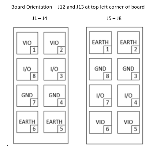 Figure 2-2 THVD4431EVM "L" Pin Header
Map
Figure 2-2 THVD4431EVM "L" Pin Header
MapThe function of each individual “L” pin depends on the mode in which the THVD4431 is being operated in.
Bus pins on the other hand are the higher voltage tolerant pins for use with RS-485 or RS-232 depending on chosen operation mode. The bus pins are accessible in a few different ways depending on mode of use. Both RS-232 and RS-485 modes have all “R” pin signals routed to an 8x2 header J14. If headers J19 and J23 are shunted, then R1 and R2 signals are available on terminal block J26. If headers J20 and J24 are shunted, then R3 and R4 signals are available on terminal block J27. If every row of header J14 is shunted, then all signals R1-R8 are available on the D-SUB connector J25. A brief summary is given in Table 3-3.
| U1 Pin | Output Option 1 | Output Option 2 | Output Option 3 | Output Option 4 |
|---|---|---|---|---|
| R1 | J14; Row 1; column 1 | J19; column 1 | J26 (if J19 is shunted) | J25 (if J14 row 1 is shunted) |
| R2 | J14; Row 2; column 1 | J23; column 1 | J26 (if J23 is shunted) | J25 (if J14 row 2 is shunted) |
| R3 | J14; Row 3; column 1 | J20; column 1 | J27 (if J20 is shunted) | J25 (if J14 row 3 is shunted) |
| R4 | J14; Row 4; column 1 | J24; column 1 | J27 (if J24 is shunted) | J25 (if J14 row 4 is shunted) |
| R5 | J14; Row 5; column 1 | J25 (if J14 row 5 is shunted) | N/A | N/A |
| R6 | J14; Row 6; column 1 | J25 (if J14 row 6 is shunted) | N/A | N/A |
| R7 | J14; Row 7; column 1 | J25 (if J14 row 7 is shunted) | N/A | N/A |
| R8 | J14; Row 8; column 1 | J25 (if J14 row 8 is shunted) | N/A | N/A |
How these pins are connected depends on the chosen operation mode and personal preference of the end user.
RS-232 Operation
With an understanding of the general architecture of the device and EVM a more thorough look at the RS-232 modes of operation is important. When entering the mode 001 for M2, M1, and M0 respectively the device enters RS-232 mode which has the transceiver setup as shown in Figure 3-3.
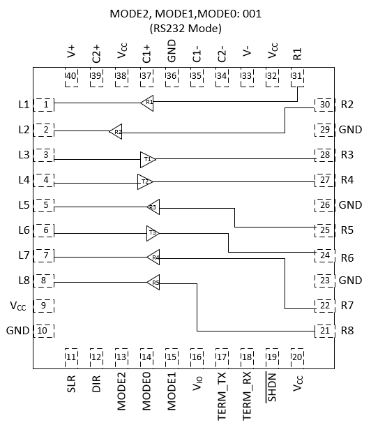 Figure 2-3 THVD4431EVM: MODE 001 (RS232
Mode)
Figure 2-3 THVD4431EVM: MODE 001 (RS232
Mode)This is commonly referred to as a 3T5R setup as there are three transmitters and 5 receivers. At an individual transceiver level, the type of RS-232 signal being transmitter or received is not important to the transceiver as the PHY layer characteristics are the same regardless of RS-232 signal type. However, the specific configuration is generally used with the following RS-232 signals: TX, RX, TRS, CTS, DSR, DTR, RI, and DCD. While this configuration of signals isn’t strictly required – most 3T5R RS-232 applications use these signals and require this configuration and if J25 (the DSUB connector) is used the pinout of the connector mimics the standard placement of the aforementioned RS-232 cables – this is summarized in Table 3-4.
| U1 Pin | Standard RS-232 Circuit Mnemonic | J25 Pin |
|---|---|---|
| R1 | DCD | 1 |
| R2 | RX | 2 |
| R3 | TX | 3 |
| R4 | DTR | 4 |
| R5 | DSR | 6 |
| R6 | RTS | 7 |
| R7 | CTS | 8 |
| R8 | RI | 9 |
Many RS-232 test plans typically require a loop back test as well. The THVD4431 integrates a RS-232 loopback mode to make this testing quick and simple. When putting the device into mode 000 for M2, M1, and M0 respectively and a logical diagram is shown in Figure 3-4.
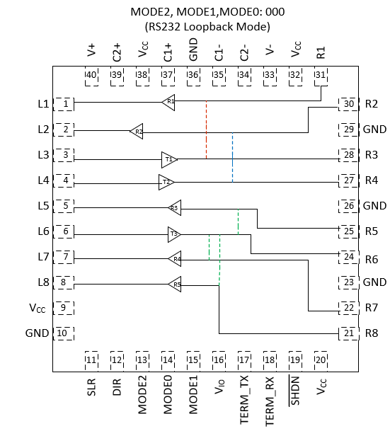 Figure 2-4 THVD4431EVM MODE 000 (RS232
Loopback Mode)
Figure 2-4 THVD4431EVM MODE 000 (RS232
Loopback Mode)RS-485 Operation
This section is a brief overview of the RS-485 operation modes. There are three different operational modes of the RS-485 portion of the transceiver: Half Duplex, Full Duplex, and RS-485 loopback mode.
Half duplex operation is a very common implementation of RS-485 and entered when the mode is 010 for M2, M1, M0 respectively. In half duplex operation, the receive and transmit pins are shared by the transceiver allowing for asynchronous bi-directional communication on two wires with the trade-off being that the bus can only have one driver at a time and a device cannot receive and transmit data simultaneously. Figure 3-5 shows the internal configuration of the THVD4431 in half duplex RS-485 mode.
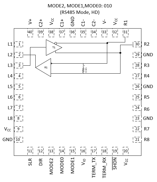 Figure 2-5 THVD4431EVM: MODE 010 (RS485
Half Duplex Mode)
Figure 2-5 THVD4431EVM: MODE 010 (RS485
Half Duplex Mode)The termination resistor shown is disabled by default. In Half-Duplex mode, TERM_RX is a don’t care value and the integrated termination is only controlled by TERM_TX. Driver input is connected to L3 and the RS-485 console side output is L2.
The next mode of operation is full duplex operation, which is mode 011 for M2, M1, M0, respectively. This mode of operation separates the driver and receiver of the RS-485 transceiver, which leads to a 4-signal wire interface. This is shown in Figure 3-6.
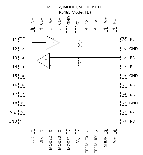 Figure 2-6 THVD4431EVM: MODE 011 (RS485
Full Duplex Mode)
Figure 2-6 THVD4431EVM: MODE 011 (RS485
Full Duplex Mode)Finally, the last RS-485 operation mode that is supported is RS-485 loopback, which is entered by mode 111 for M2, M1, M0, respectively. This mode shorts the driver output to the receiver inputs to allow for diagnostic testing of the THVD4431 as shown in Figure 3-7.
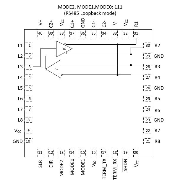 Figure 2-7 THVD4431EVM: MODE 111(RS485
Loopback Mode)