SLOS626B December   2009  – November 2015 TPA2011D1

PRODUCTION DATA.  

  1. Features
  2. Applications
  3. Description
  4. Revision History
  5. Device Comparison Table
  6. Pin Configuration and Functions
  7. Specifications
    1. 7.1 Absolute Maximum Ratings
    2. 7.2 ESD Ratings
    3. 7.3 Recommended Operating Conditions
    4. 7.4 Thermal Information
    5. 7.5 Electrical Characteristics
    6. 7.6 Operating Characteristics
    7. 7.7 Dissipation Ratings
    8. 7.8 Typical Characteristics
  8. Parameter Measurement Information
  9. Detailed Description
    1. 9.1 Overview
    2. 9.2 Functional Block Diagram
    3. 9.3 Feature Description
      1. 9.3.1 Fully Differential Amplifier
        1. 9.3.1.1 Advantages of Fully Differential Amplifiers
      2. 9.3.2 Eliminating the Output Filter With the TPA2011D1
        1. 9.3.2.1 Effect on Audio
        2. 9.3.2.2 When to Use an Output Filter
      3. 9.3.3 Short Circuit Auto-Recovery
      4. 9.3.4 Integrated Image Reject Filter for DAC Noise Rejection
    4. 9.4 Device Functional Modes
      1. 9.4.1 Summing Input Signals With the TPA2011D1
        1. 9.4.1.1 Summing Two Differential Input Signals
        2. 9.4.1.2 Summing a Differential Input Signal and a Single-Ended Input Signal
        3. 9.4.1.3 Summing Two Single-Ended Input Signals
      2. 9.4.2 Shutdown Mode
  10. 10Application and Implementation
    1. 10.1 Application Information
    2. 10.2 Typical Applications
      1. 10.2.1 TPA2011D1 with Differential Input
        1. 10.2.1.1 Design Requirements
        2. 10.2.1.2 Detailed Design Procedure
          1. 10.2.1.2.1 Input Resistors (RI)
          2. 10.2.1.2.2 Decoupling Capacitor (CS)
        3. 10.2.1.3 Application Curves
      2. 10.2.2 TPA2011D1 with Differential Input and Input Capacitors
        1. 10.2.2.1 Design Requirements
        2. 10.2.2.2 Detailed Design Procedure
          1. 10.2.2.2.1 Input Capacitors (CI)
        3. 10.2.2.3 Application Curves
      3. 10.2.3 TPA2011D1 with Single-Ended Input
        1. 10.2.3.1 Design Requirements
        2. 10.2.3.2 Detailed Design Procedure
        3. 10.2.3.3 Application Curves
  11. 11Power Supply Recommendations
    1. 11.1 Power Supply Decoupling Capacitors
  12. 12Layout
    1. 12.1 Layout Guidelines
    2. 12.2 Layout Example
  13. 13Device and Documentation Support
    1. 13.1 Community Resources
    2. 13.2 Trademarks
    3. 13.3 Electrostatic Discharge Caution
    4. 13.4 Glossary
  14. 14Mechanical, Packaging, and Orderable Information

6 Pin Configuration and Functions

YFF Package
9-Pin DSBGA
Top View
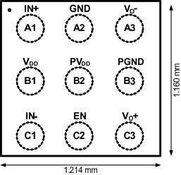
TPA2011D1 pin_los626.gif

Pin Functions

PIN I/O DESCRIPTION
NAME NO.
EN C2 I Shutdown terminal. When terminal is low the device is put into Shutdown mode.
GND A2 I Analog ground terminal. Must be connected to same potential as PGND using a direct connection to a single point ground.
IN– C1 I Negative differential audio input
IN+ A1 I Positive differential audio input
PGND B3 I High-current Analog ground terminal. Must be connected to same potential as GND using a direct connection to a single point ground.
PVDD B2 I High-current Power supply terminal. Must be connected to same power supply as VDD using a direct connection. Voltage must be within values listed in Recommended Operating Conditions table.
VDD B1 I Power supply terminal. Must be connected to same power supply as PVDD using a direct connection. Voltage must be within values listed in Recommended Operating Conditions table.
VO- A3 O Negative BTL audio output
VO+ C3 O Positive BTL audio output