SLOS841B September 2013 – January 2015 TPA3131D2 , TPA3132D2
PRODUCTION DATA.
- 1 Features
- 2 Applications
- 3 Description
- 4 Revision History
- 5 Pin Configuration and Functions
- 6 Specifications
-
7 Detailed Description
- 7.1 Overview
- 7.2 Functional Block Diagram
- 7.3
Feature Description
- 7.3.1 Gain Setting and Master and Slave
- 7.3.2 Input Impedance
- 7.3.3 Start-up/Shutdown Operation
- 7.3.4 PLIMIT Operation
- 7.3.5 GVDD Supply
- 7.3.6 BSPx and BSNx Capacitors
- 7.3.7 Differential Inputs
- 7.3.8 Device Protection System
- 7.3.9 DC Detect Protection
- 7.3.10 Short-Circuit Protection and Automatic Recovery Feature
- 7.3.11 Thermal Protection
- 7.3.12 Efficiency: LC Filter Required with the Traditional Class-D Modulation Scheme
- 7.3.13 Ferrite Bead Filter Considerations
- 7.3.14 When to Use an Output Filter for EMI Suppression
- 7.3.15 AM Avoidance EMI Reduction
- 7.4 Device Functional Modes
- 8 Applications and Implementation
- 9 Power Supply Recommendations
- 10Layout
- 11Device and Documentation Support
- 12Mechanical, Packaging, and Orderable Information
6 Specifications
6.1 Absolute Maximum Ratings
over operating free-air temperature range (unless otherwise noted)| MIN | MAX | UNIT | ||
|---|---|---|---|---|
| Supply voltage, VCC | PVCC, AVCC | –0.3 | 30 | V |
| Input voltage, VI | INPL, INNL, INPR, INNR | –0.3 | 6.3 | V |
| PLIMIT, GAIN / SLV, SYNC | –0.3 | GVDD+0.3 | V | |
| AM0, AM1, AM2, MUTE, SDZ | –0.3 | PVCC+0.3 | V | |
| Slew rate, maximum | AM0, AM1, AM2, MUTE, SDZ | 10 | V/ms | |
| Operating free-air temperature, TA | –40 | 85 | °C | |
| Operating junction temperature, TJ | –40 | 150 | °C | |
| Storage temperature, Tstg | –40 | 125 | °C | |
6.2 ESD Ratings
| VALUE | UNIT | |||
|---|---|---|---|---|
| V(ESD) | Electrostatic discharge | Human-body model (HBM), per ANSI/ESDA/JEDEC JS-001(1) | ±2000 | V |
| Charged-device model (CDM), per JEDEC specification JESD22-C101(2) | ±500 | |||
(1) JEDEC document JEP155 states that 500-V HBM allows safe manufacturing with a standard ESD control process.
(2) JEDEC document JEP157 states that 250-V CDM allows safe manufacturing with a standard ESD control process.
6.3 Recommended Operating Conditions
over operating free-air temperature range (unless otherwise noted)| MIN | NOM | MAX | UNIT | ||||
|---|---|---|---|---|---|---|---|
| VCC | Supply voltage | PVCC, AVCC | 4.5 | 26 | V | ||
| VIH | High-level input voltage | AM0, AM1, AM2, MUTE, SDZ, SYNC | 2 | V | |||
| VIL | Low-level input voltage | AM0, AM1, AM2, MUTE, SDZ, SYNC | 0.8 | V | |||
| VOL | Low-level output voltage | FAULTZ, RPULL-UP = 100 kΩ, PVCC = 26 V | 0.8 | V | |||
| IIH | High-level input current | AM0, AM1, AM2, MUTE, SDZ (VI = 2 V, VCC = 18 V) | 50 | µA | |||
| RL(BTL) | Minimum load Impedance | Output filter: L = 10 µH, C = 680 nF | 3.2 | 4 | Ω | ||
| RL(PBTL) | Output filter: L = 10 µH, C = 1 µF | 1.6 | |||||
| Lo | Output-filter Inductance | Minimum output filter inductance under short-circuit condition | 1 | µH | |||
6.4 Thermal Information
| THERMAL METRIC(1)(2) | TPA313xD2 | UNIT | ||
|---|---|---|---|---|
| VQFN | ||||
| 32 PINS | ||||
| RθJA | Junction-to-ambient thermal resistance | 31.3 | °C/W | |
| ψJT | Junction-to-top characterization parameter | 0.2 | ||
| ψJB | Junction-to-board characterization parameter | 5.5 | ||
(1) For more information about traditional and new thermal metrics, see the IC Package Thermal Metrics application report, SPRA953.
(2) The heat sink drawing used for the thermal model data are shown in the application section, size: 14mm wide, 50mm long, 25mm high.
6.5 DC Electrical Characteristics
TA = 25°C, AVCC = PVCC = 7.4 V to 26 V, RL = 8 Ω (unless otherwise noted)6.6 AC Electrical Characteristics
TA = 25°C, AVCC = PVCC = 7.4 V to 24 V, RL = 8 Ω (unless otherwise noted)| PARAMETER | TEST CONDITIONS | MIN | TYP | MAX | UNIT | |
|---|---|---|---|---|---|---|
| KSVR | Power supply ripple rejection | 200 mVPP ripple at 1 kHz, Gain = 20 dB, Inputs AC-coupled to GND | –70 | dB | ||
| PO | Continuous output power | RL = 8 Ω, THD+N = 10%, f = 1 kHz, PVCC = 7.4 V (TPA3131D2) | 4 | W | ||
| RL = 4 Ω, THD+N = 10%, f = 1 kHz, PVCC = 7.4 V (TPA3131D2) | 7.3 | |||||
| RL = 8 Ω, THD+N = 10%, f = 1 kHz, PVCC = 19V (TPA3132D2) | 25 | |||||
| RL = 4 Ω, THD+N = 10%, f = 1 kHz, PVCC = 19V (TPA3132D2) | 42 | |||||
| THD+N | Total harmonic distortion + noise | RL = 8 Ω, f = 1 kHz, PO = 0.1W to 2 W (TPA3132D2) RL = 8 Ω, f = 1 kHz, PO = 0.1W to 12.5 W (TPA3131D2) |
0.1% | |||
| Vn | Output integrated noise | 20 Hz to 22 kHz, A-weighted filter, Gain = 20 dB | 70 | µV | ||
| –80 | dBV | |||||
| Crosstalk | VO = 1 Vrms, Gain = 20 dB, f = 1 kHz | –100 | dB | |||
| SNR | Signal-to-noise ratio | Maximum output at THD+N < 1%, f = 1 kHz, Gain = 20 dB, A-weighted (TPA3131D2, PVCC = 7.4V) | 98 | dB | ||
| Maximum output at THD+N < 1%, f = 1 kHz, Gain = 20 dB, A-weighted (TPA3131D2, PVCC = 19V) | 105 | |||||
| fOSC | Oscillator frequency | AM2=0, AM1=0, AM0=0 | 376 | 400 | 424 | kHz |
| AM2=0, AM1=0, AM0=1 | 470 | 500 | 530 | |||
| AM2=0, AM1=1, AM0=0 | 564 | 600 | 636 | |||
| AM2=0, AM1=1, AM0=1 | 940 | 1000 | 1060 | |||
| AM2=1, AM1=0, AM0=0 | 1128 | 1200 | 1278 | |||
| AM2=1, AM1=0, AM0=1 | Reserved | |||||
| AM2=1, AM1=1, AM0=0 | ||||||
| AM2=1, AM1=1, AM0=1 | ||||||
| Thermal trip point | 150+ | °C | ||||
| Thermal hysteresis | 15 | °C | ||||
| Over current trip point | TPA3131D2 | 3.4 | A | |||
| TPA3132D2 | 7 | |||||
6.7 Typical Characteristics
fs = 400 kHz (unless otherwise noted)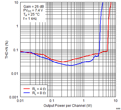 Figure 1. Total Harmonic Distortion + Noise (BTL) vs Output Power
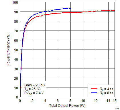 Figure 3. Power Efficiency (BTL) vs Supply Voltage
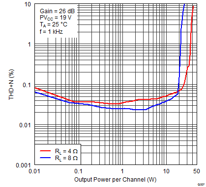 Figure 5. Total Harmonic Distortion + Noise (BTL) vs Output Power
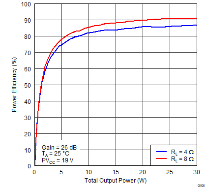 Figure 7. Power Efficiency (BTL) vs Output Power
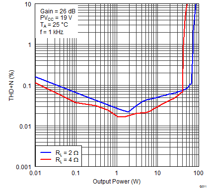 Figure 9. Total Harmonic Distortion + Noise (TPA3132D2 PBTL) vs Output Power
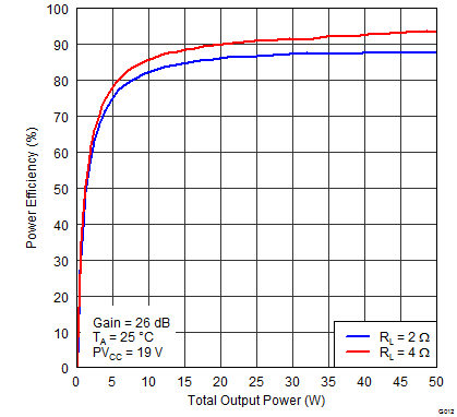 Figure 11. Power Efficiency (TPA3132D2 PBTL) vs Output Power
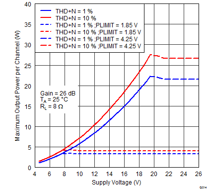 Figure 15. Maximum Output Power (BTL) vs Supply Voltage
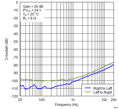 Figure 17. Crosstalk (BTL) vs Frequency
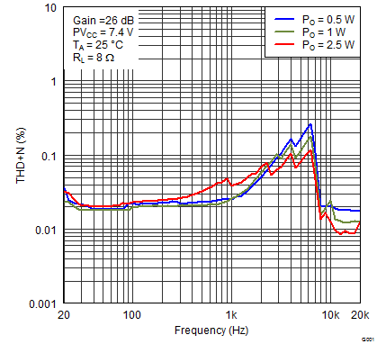 Figure 2. Total Harmonic Distortion + Noise (BTL) vs Frequency
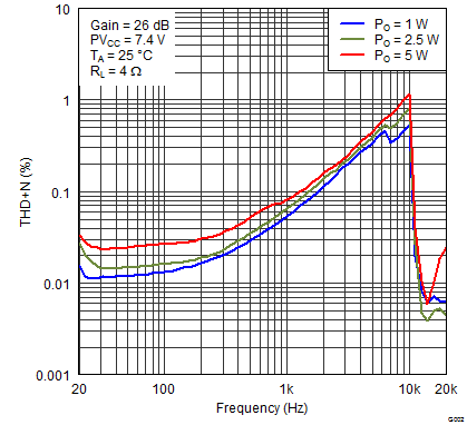 Figure 4. Total Harmonic Distortion + Noise (BTL) vs Frequency
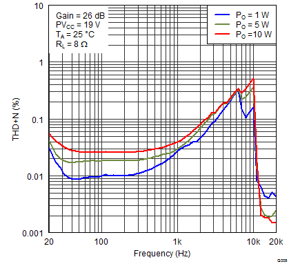 Figure 6. Total Harmonic Distortion + Noise (BTL) vs Frequency
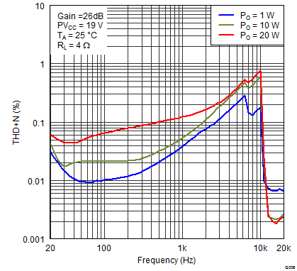 Figure 8. Total Harmonic Distortion + Noise (BTL) vs Frequency
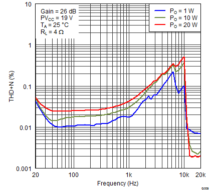 Figure 10. Total Harmonic Distortion + Noise (TPA3132D2 PBTL) vs Frequency
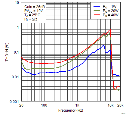 Figure 12. Total Harmonic Distortion + Noise (TPA3132D2 PBTL) vs Frequency
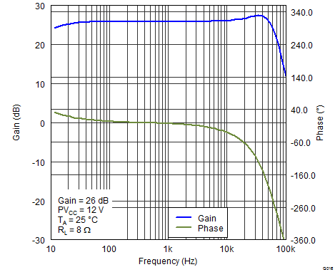 Figure 14. Gain/Phase (BTL) vs Frequency
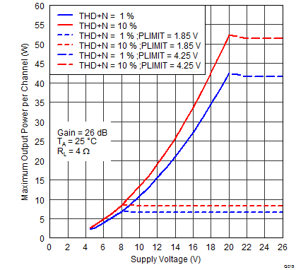 Figure 16. Maximum Output Power (BTL) vs Supply Voltage
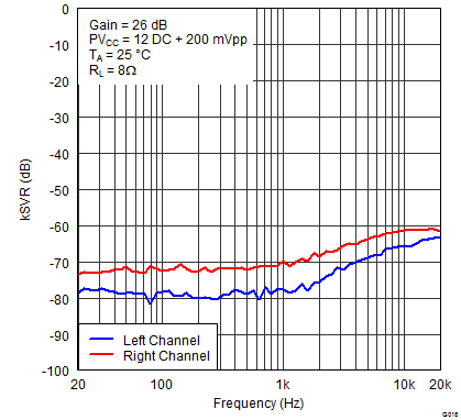 Figure 18. PSRR vs Frequency
