SLUAA69 July 2020 – MONTH TPS548D22
6.4 Startup Waveforms and Behaviors Analysis after the First OVP
Figure 6-6, Figure 6-7, Figure 6-8 and Figure 6-9 show waveforms after the first OVP with details.
The corresponding circuit behaviors of each stage are shown in Figure 6-10, Figure 6-11, Figure 6-12, Figure 6-13, Figure 6-14, and Figure 6-15.
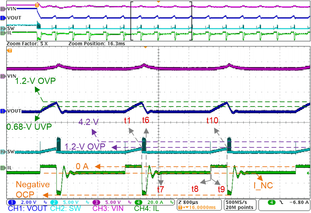 Figure 6-6 Start-up Waveforms after the First OVP with Details: 1
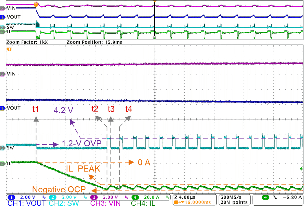 Figure 6-7 Start-up Waveforms after the First OVP with Details: 2
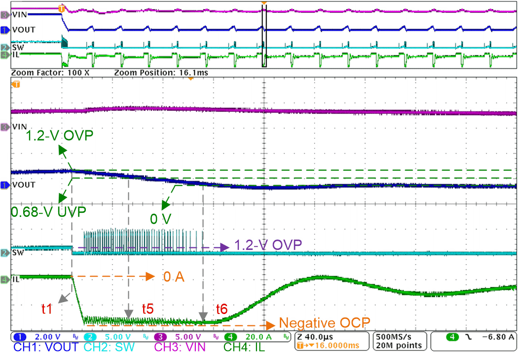 Figure 6-8 Start-up Waveforms after the First OVP with Details: 3
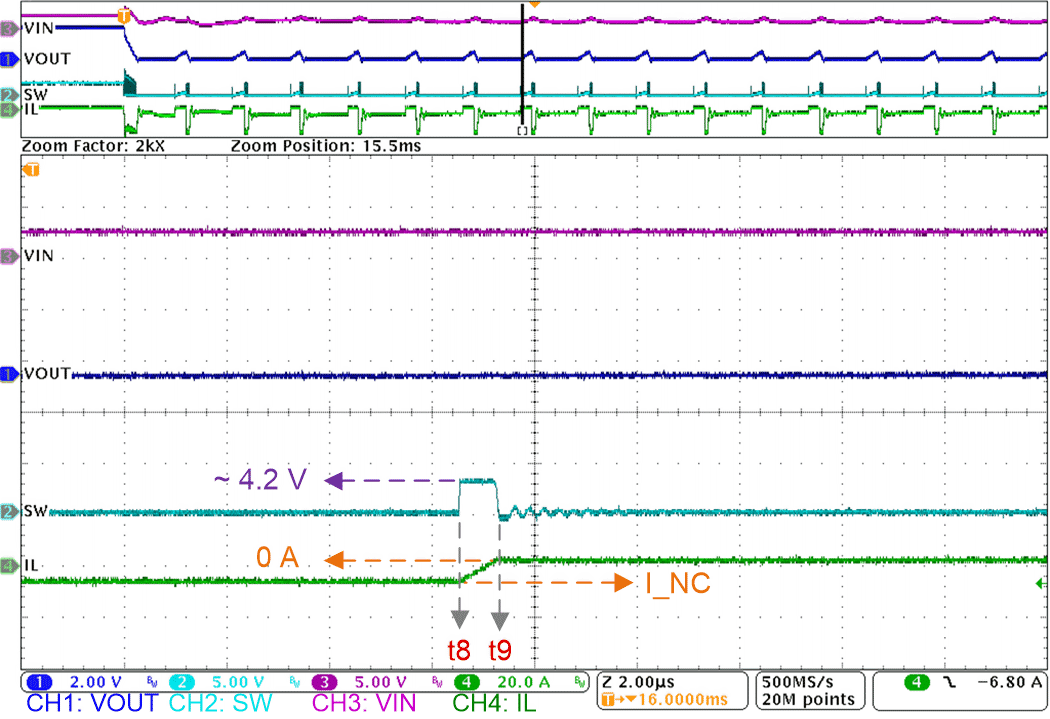 Figure 6-9 Start-up Waveforms after the First OVP with Details: 4
From t1 to t2, OVP is triggered at t1. The high-side MOSFET keeps turning OFF and the low-side MOSFET keeps turning on to discharge the output until t2, at which time the negative current limit (negative OCP) is reached. Correspondingly, the output voltage drops, the SW voltage stays at 0 V and the inductor current increases in the negative direction during t1 to t2.
From t2 to t6, negative OCP is first reached at t2. Then the low-side MOSFET driver is turned off, and the high-side MOSFET driver is turned on for a minimum on-time to limit the inductor current so that it does not exceed the negative limit level. With the high-side MOSFET turning on for a minimum on-time (t2 to t3), the inductor current flows in the positive direction but still in the negative region. After the minimum on-time, the low-side MOSFET turns on and the high-side MOSFET turns off. The inductor current continues flowing in the negative direction (t3 to t4) and reaches the negative current limit again (negative OCP is triggered again) at t4. This cycle will continue until negative OCP is not triggered anymore at t6. At this time, the output voltage is close to being completely discharged. The high-side MOSFET stays turned off and the low-side MOSFET stays turned on until the 1 ms UVP delay is completed. Note that at t5, UVP is reached, but the internal 1 ms UVP delay time counter does not begin counting since the soft-start operation is not completed. This is discussed in Start-up Waveforms and Behaviors Analysis Overview.
From t6 to t7, the output capacitor is completely discharged and voltage across the inductor is zero at t6. As there is no voltage across the inductor to maintain the current, it starts to fall but still keep flowing in the original direction to charge the output capacitor with the opposite polarity. Then, the capacitor starts to discharge again back through the coil and the whole process is repeated. The polarity of the voltage changes as the energy is passed back and forth between the capacitor and inductor producing a LC oscillator and finally decays the oscillations to zero at t7 due to some energy losses.
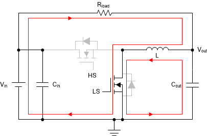 Figure 6-10 t1~t2: OVP triggers, output discharge until reaching negative OCP
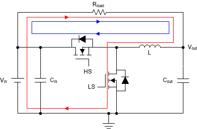 Figure 6-11 t2~t6: High-side MOSFET turns on for a minimum on-time
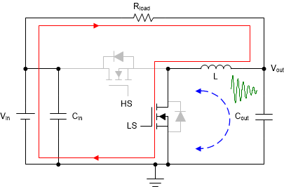 Figure 6-12 t6~t7: LC resonating, output voltage follows resonating
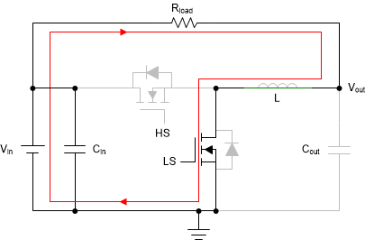 Figure 6-13 t7~t8: Output voltage is 0V, inductor behaves as a pure wire
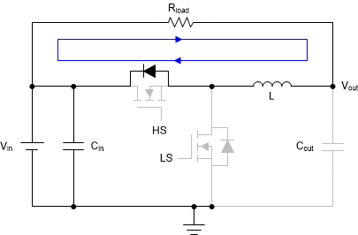 Figure 6-14 t8~t9: Inductor current is freewheeling through high-side body diode
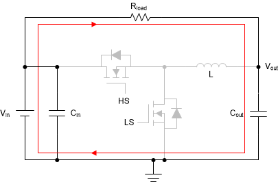 Figure 6-15 t9~t10: Output capacitor charging and OVP is
triggered again
Figure 6-15 t9~t10: Output capacitor charging and OVP is
triggered againFrom t7 to t8, energy stored in the LC oscillator is fully discharged at t7. The inductor is equivalent to a short circuit. The whole circuit is a pure resistance circuit with a constant negative current with Vout/Rload through the inductor.
From t8 to t9, the 1 ms UVP delay is completed at t8, the device turns OFF both high-side and low-side MOSFETs drivers. However, there still is current left in the inductor and the current cannot suddenly change. The freewheeling current of the inductor continues to flows through the body diode of the high-side MOSFET and decays to zero. The corresponding SW node voltage roughly equals to the input voltage.
From t9 to t10, the output capacitor is charged again only through the load path. This results in the output voltage ramping up and OVP being triggered again at t10 (repeat as t1). A new OVP cycle begins. Also note that the SW voltage exactly follows the output voltage since there has no current flowing in the inductor.
The waveform analysis explains why the OVP event is cyclically triggered and yields a system start-up issue. Apart from that, some other behaviors, such as intense fluctuation of the input voltage, possible inductor saturation and MOSFET damage cannot be accepted for actual power supply application.