SLUAA84A January 2021 – February 2022 BQ769142 , BQ76942 , BQ76952
7 Controlling LD
With a high-side FET design the LD pin will normally connect to PACK+ and is used for a drive reference for DSG, for a wake-up signal, and for current recovery if selected. The data sheet indicates that when the driver is not used LD may be tied to PACK+ through a resistor or may be pulled to VSS. If pulled high it will prevent the part from entering shutdown. If connected to VSS it cannot be used to control current recovery. An MCU could recover the OCD event using the host command. Since the device provides a pullup to test for load removal, a circuit can be designed to control LD if desired. The MCU could control the circuit if not providing recovery by command, or if no MCU is available it could be controlled by the PACK- pin level as shown in Figure 7-1. When a load is present on the PACK terminals after a fault which holds the PACK- near PACK+, LD is held low. If configured appropriately recovery from the current fault is prevented. The circuit provides a pulldown on the PACK-, if the load is removed such that this pulldown can turn off the signal FET Q32, LD will be released and the BQ769x2 will pull LD high allowing current recovery. Note that the circuit will provide a pulldown on PACK- which will tend to keep the PACK voltage near normal levels, this will be a leakage on the battery while the load is present on the PACK terminals. When CHG remains on, the gate drive voltage will pull up the PACK- voltage and may prevent turn off of Q32 depending on the values of the R66 and R67 resistors.
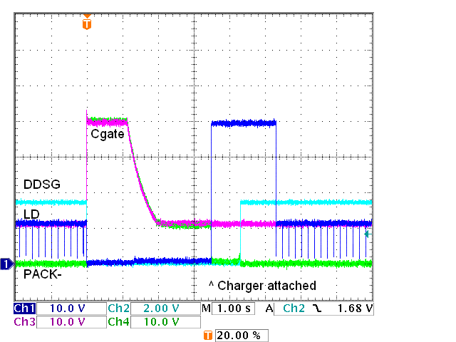
Figure 7-2 shows an OCD event with the test circuit. DDSG is turned off, the load pulls PACK- up, LD is pulled down by the circuit. The charge FET gate Cgate is also pulled up by PACK- and discharges to the PACK- level over time. When the load is released but the part stays awake with DCHG on, the driver biases up PACK- to near the driver level. Depending on the divider resistors selected for R66 and R67 the circuit may hold LD low, and recovery will not occur until a charger is attached as shown in Figure 7-3. When the BQ769x2 is asleep, if CHG is off during sleep the PACK- can fall after the load is removed and recovery may happen quickly as shown in Figure 7-4. If the load is removed after the current stops after the Protections:Load Detect:Active Time, the part will retry after the Protections:Load Detect:Retry Delay as shown in Figure 7-5. If necessary the part will retry until the Protections:Load Detect:Timeout.
 Figure 7-2 OCD with LD
Controlled
 Figure 7-4 OCD During Sleep with
Recovery
 Figure 7-3 OCD with Recovery From
Charger Connection
 Figure 7-5 OCD During Sleep with
Recovery On Retry
Figure 7-5 OCD During Sleep with
Recovery On RetryWith low-side switching and LD tied to VSS or LD controlled by the cirucit above, wake-up will need to come from TS2. A simple circuit to do this is shown in Figure 7-6. When the "Wake" signal is pulled up toward PACK+, TS2 is pulled down causing the BQ769x2 to wake up. If the WAKE signal is connected to PACK+ directly, the circuit will provide a continuous drain on the battery. Adjust the value of R80 and provide transient protection as needed or use an alternate circuit suitable for the application.