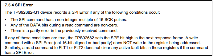
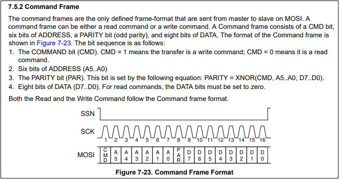
TPS92682-Q1 Frame Definitions and Examples
Trademarks
TI E2E are trademarks of Texas Instruments.
All trademarks are the property of their respective owners.
1 Build a Frame
Create a valid frame based on address and data with parity.
Uint16 assembleSPICmd_682(Uint16 write, Uint16 address, Uint8 data)
{
    Uint16 assembledCmd = 0; // Build this to shift through parity calculation
    Uint16 parity = 0;       // Parity bit calculated here
    Uint16 packet = 0;       // This will be what we send

    if(write)
    {
        assembledCmd |= 0x8000;  // Set CMD = 1
    }

    assembledCmd |= (((address << 9) & 0x7E00) | (Uint16)(data & 0x00FF));
    packet = assembledCmd;

    // Calculate parity
    while(assembledCmd > 0)
    {
        // Count the number of 1s in the LSb
        if(assembledCmd & 0x0001)
        {
            parity++;
        }
        // Shift right
        assembledCmd >>= 1;
    }

    // If the LSb is a 0 (even # of 1s), we need to add the odd parity bit
    if(!(parity & 0x0001))
    {
        packet |= (1 << 8);
    }

    return(packet);
}
2 Response Frame
The command response frames are defined in the following portions of the TPS92682-Q1 Dual-Channel Constant-Voltage and Constant-Current Controller with SPI Data Sheet.
The following image illustrates the read response frame section of the data sheet.

The command frame (Build a Frame) is SPI MOSI and the response is found in SPI MISO following it. The SPI MOSI command issued = 0x23 0x00. In this example the return (MISO result of 2 reads per SPI) has a status byte of 0x60 with a data byte of 0x02 indicating: CH2UV: Output undervoltage fault (CH2UV is disabled if 2PH is set to '1'). For a detailed explanation of the expected SPI bus return value with the TPS92682-Q1, visit the TI E2E™ support forum.
The following image shows the Read Fault Register 0x11 (FLT1).

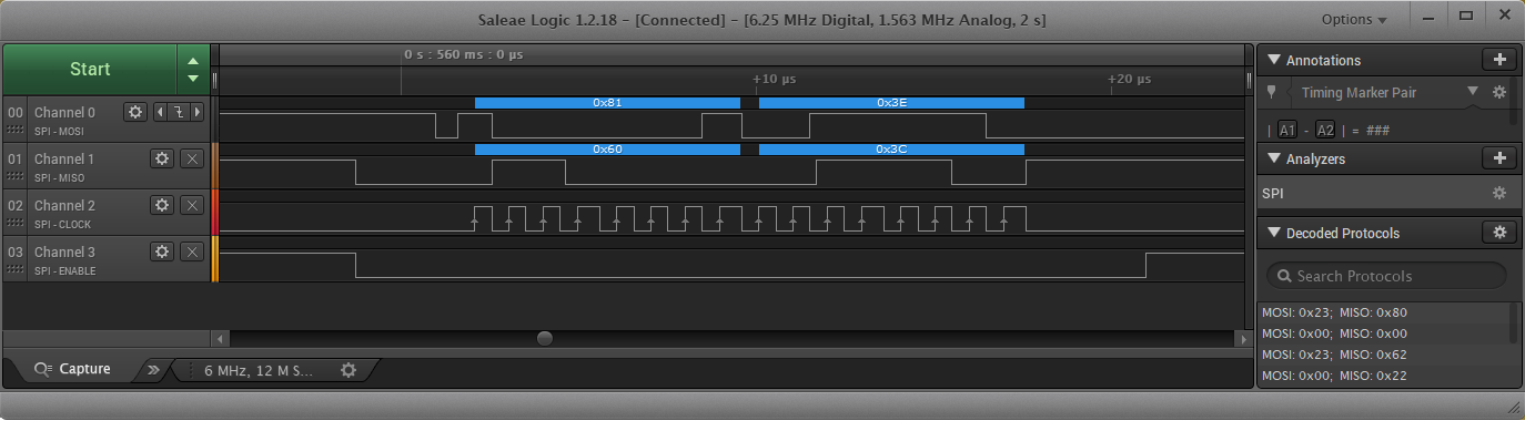
The following image shows the write response frame format, write error/POR frame format SPI error sections from the data sheet:

The following command frame is SPI MOSI and the response is found in SPI MISO after it. The SPI MOSI command issued = 0x81 0x3E. In this example, the return (MISO result of previous read of register 0x00) has a status byte of 0x60 with a data byte of 0x3c indicating: default power up value for register 0x00. For a detailed explanation of the expected SPI bus return value with the TPS92682-Q1, visit the TI E2E™ support forum.
The following image shows the Write Enable Register 0x00 (EN).