SLUAAQ5 May 2024 BQ769142 , BQ76942 , BQ76952 , BQ76972
- 1
- Abstract
-
1 General Operation FAQs
- 1.1 What are the differences between the devices in the BQ769x2 family?
- 1.2 What are the differences between the BQ769x0 and BQ769x2 device families?
- 1.3 Do I need a microcontroller to control the device or can the device run autonomously?
- 1.4 What is the minimum number of cells required to operate the device and how to connect them?
- 1.5 Can the device perform gauging to calculate State of Health (SOH) and State of Charge (SOC)?
- 1.6 How does unused pins needs to be connected?
- 1.7 What does support random cell attachment means?
- 1.8 How do I RESET the BQ769x2 device?
- 1.9 How does the BQ769x2 recover from a fault?
- 1.10 Does the BQ769x2 support open wire detection?
-
2 Control FETs FAQs
- 2.1 What are the tradeoffs of High side vs Low side gate driving?
- 2.2 Can the BQ769x2 be used for low-side FET driving?
- 2.3 Is the CP1 capacitor necessary for low-side switching?
- 2.4 How long does the BQ769x2 take to turn on the FETs on power up?
- 2.5 What are the typical voltages for the Charge (CHG) and Discharge (DSG) pins?
- 2.6 What are the voltage ranges of the Precharge (PCHG) and Predischarge (PDSG) pins?
- 2.7 How can I achieve faster gate turn-offs for DSG?
- 2.8 Why are the FETs turning OFF while data memory registers are being configured in CONFIG_UPDATE mode?
- 2.9 Is there a way to manually control PCHG and PDSG?
- 2.10 Can I use an NFET with the PDSG pin?
- 2.11 What states are PDSG and PCHG when disabled?
- 2.12 How do I disable the Discharge FET (DFET) and Charge FET (CFET)?
- 2.13 Can the BQ769x2 idle with PDSG ON during SLEEP mode?
-
3 Coulomb Counter (CC) and ADCs FAQs
- 3.1 What resolution does the ADC provide for voltage measurement?
- 3.2 How fast does the BQ769x2 ADC sample?
- 3.3 How does the ADC operates while on SLEEP mode?
- 3.4 Does the coulomb counter provide a SoC and SoH measurement?
- 3.5 Can the coulomb counter be used to measure instantaneous current?
- 3.6 What is the resolution of the coulomb counter?
- 3.7 Is the coulomb counter used for overcurrent detection?
- 3.8 What is the difference between OCD1, OCD2, OCD3, and SCD?
- 3.9 Why is the accumulated charge measurement seems to be producing an incorrect value?
- 3.10 Why is the voltage of CELL1 seems to be measuring incorrectly?
-
4 Communication Protocols and Programming FAQs
- 4.1 What communication protocols does the BQ769x2 support?
- 4.2 Does the BQ769x2 support cyclic redundancy checking (CRC)?
- 4.3 Does the I 2 C lines require pull-up resistors to operate?
- 4.4 Does the BQ769x2 support clock stretching?
- 4.5 Does the BQ769x2 allow block writes and reads?
- 4.6 Does the BQ769x2 require isolation to communicate?
- 4.7 When shall I use OTP programming?
- 4.8 How does the BQ769x2 OTP memory work?
- 4.9 How many times can the BQ769x2 OTP memory be modified?
- 4.10 What hardware is necessary to program the OTP memory?
- 4.11 How can the host reset the ALERT pin interrupt?
- 4.12 Why is my subcommand returning incorrect data?
-
5 Calibration and Temperature Sensing FAQs
- 5.1 Does the BQ769x2 come calibrated or do I need to calibrate externally?
- 5.2 Can custom calibrations be stored onto the BQ769x2?
- 5.3 How do I modify RAM registers to update calibrations?
- 5.4 Can each cell measurement have a custom (offset/gain) calibration factor?
- 5.5 How to configure a multipurpose pin to work as a thermistor ?
- 5.6 How many thermistors does the device support?
- 5.7 Can thermal protections be disabled and are thermistors necessary for operation?
- 5.8 Why do I need a capacitor across each thermistor?
- 5.9 How are the thermistor coefficients calculated for temperature calibration?
- 5.10 Why is the thermistor coefficient calculator tool throwing errors?
-
6 Cell Balancing FAQs
- 6.1 How does cell balancing work?
- 6.2 Can all battery cells be balanced simultaneously?
- 6.3 Does the BQ769x2 support adjacent cell balancing?
- 6.4 How does cell balancing work in RELAX mode?
- 6.5 Does the BQ769x2 support external balancing?
- 6.6 How large can the current sense resistors be at the VCx input pins?
- 6.7 Does cell balancing affect voltage measurement?
- 6.8 Why are the cells balancing for different amount of times?
-
7 Device Power and State Switching FAQs
- 7.1 What is the maximum voltage of battery packs this device support?
- 7.2 What is the maximum battery pack voltage allowed when using the charge pump?
- 7.3 Is necessary to tie BAT- to VSS?
- 7.4 How my other signal GNDs needs to be connected to PACK-?
- 7.5 Does a capacitor needs to be placed between VC0 and VC1?
- 7.6 What are the recommended typical passive components values for my schematic design?
- 7.7 How much current can the two programmable LDOs provide?
- 7.8 Can the LDO input transistor be connected to a lower voltage cell on the pack than BAT+ to increase efficiency?
- 7.9 In reference designs, why are two capacitors placed between VC16 and PACK+ as well as PACK+ and PACK-?
- 7.10 What are the different low power modes of the BQ769x2 device family?
- 7.11 How can an MCU know the BQ769x2 is in shutdown?
- 7.12 Is disabling the SHUTDOWN mode possible?
- 7.13 How does the BQ769x2 exit SHUTDOWN mode?
- 7.14 What is soft SHUTDOWN? How can I exit soft SHUTDOWN mode?
-
8 Evaluation Modules and BQStudio FAQs
- 8.1 Does the BQ769x2 family have any EVMs?
- 8.2 How much current the EVM consume while operating?
- 8.3 Can I reduce the number of cells enabled on the EVM?
- 8.4 Can multiple EVMs connect to one computer when stacking multiple EVMs?
- 8.5 Can the device interface with both SMBus and SPI at the same time?
- 8.6 Why is BQStudio not detecting to the BQ769x2EVM?
-
9 Additional Instructional Material
- 9.1 How do I access functional safety documents such as a FMEDA and pin FMEA?
- 9.2 Is there any microcontroller code examples for the BQ769x2?
- 9.3 Are there any reference designs for the BQ769x2?
- 9.4 Is there any documentation on stacking multiple BQ769x2 devices?
- 9.5 Where can I find training videos to learn more about battery monitors and protectors?
- 10References
2.7 How can I achieve faster gate turn-offs for DSG?
There are two general methods for reducing gate turn-off times.
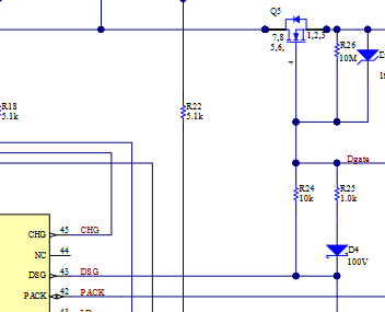
The first is shown in Figure 2-1 and offers a low cost design to speed up the turn-off by using a diode (D4) to provide a lower resistance path for the gate of the FET to discharge the stored charge compared to the turn on path. By varying the resistance, the time to turn-off can be increased or decreased as desired.
 Figure 2-1 First Speed Up Configuration
Utilizing a Single Diode (D4)
Figure 2-1 First Speed Up Configuration
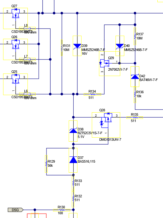
Utilizing a Single Diode (D4)The second is shown in Figure 2-2. This circuit uses the ability to drive the PMOS low quicker to provide an alternate path for the charge of the FETs to drain from the gate and into PACK+. This configuration, while more expensive, is an excellent choice for situations where multiple FETs are in parallel due to the ability to get a lower resistance. If the user is using only one or two FETs, option one is more cost efficient.
 Figure 2-2 The Second Configuration For
Multi-FET Applications using a PMOS and Diode (D37 and Q28)