SLUAAU4 June 2024 UCC28750
5 Common Issues
The Flyback Aux Winding OVP and UVLO Fault Sensing Design and Troubleshooting Tips, application note introduces several common issues and troubleshooting tips, and this section also adds some issues.
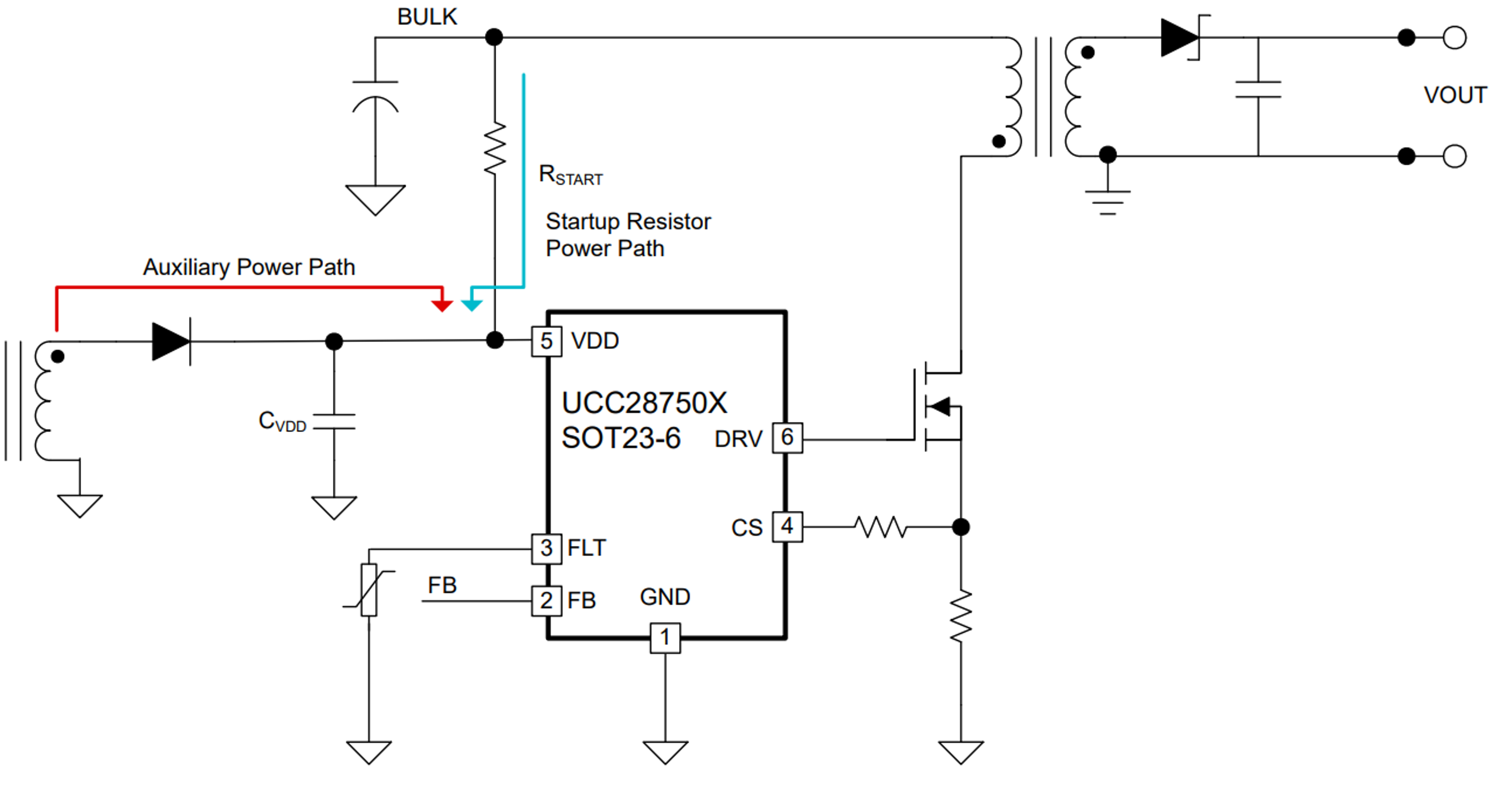
- The VDD pin is typically powered
through a resistor network connected to the rectified bulk voltage and later an
auxiliary winding in an AC/DC flyback application, and the charging path as
Figure 5-1 showing.
However, the resistor brings extra power consumption then impacts the no load power consumption, so the resistance is up to MΩ, but the side effect is that the charger current is smaller then impacts the startup time.
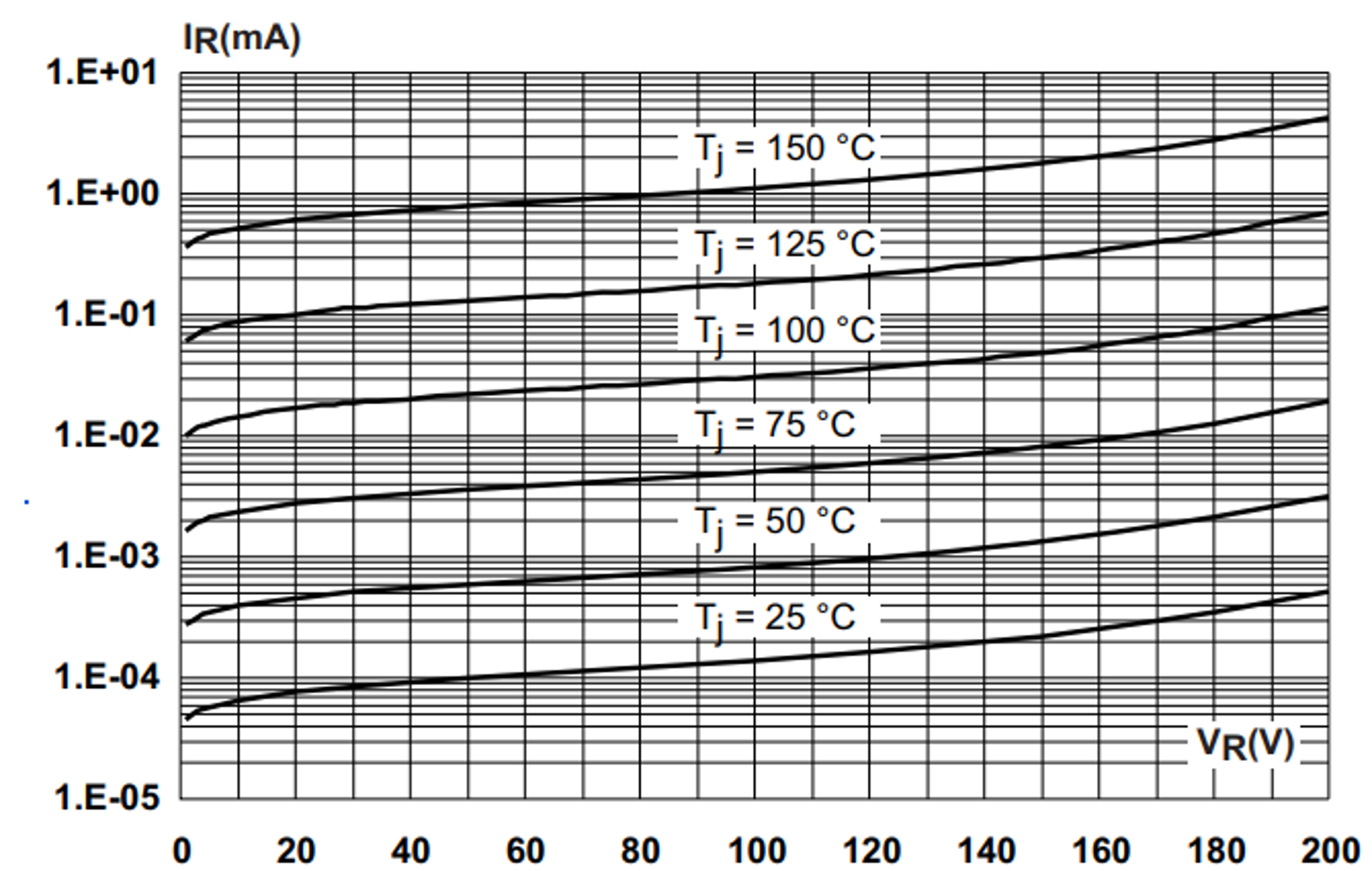
The diode at auxiliary power path has reverse current, and the reverse current increased up to 1000 times at high ambient temperature as Figure 5-2 showing, and the reverse current can also limit the charge current from resistor power path, so customer sometimes faces that the VDD can't be charged up to startup point during burn in testing, then controller can't start switching. - In the Auxpower application, the flyback has multi-output for different loading, so the cross regulation is important, TI also published the Adding a single capacitor to improve cross-regulation in dual-output flyback power supplies, technical article and also Multiple Output Flybacks: How to Improve Cross Regulation training video to guide.
- Customers can mention that the
power consumption is too high during no load testing. However, the EVM test
result is around 100mW. Customers measured higher power consumption because the
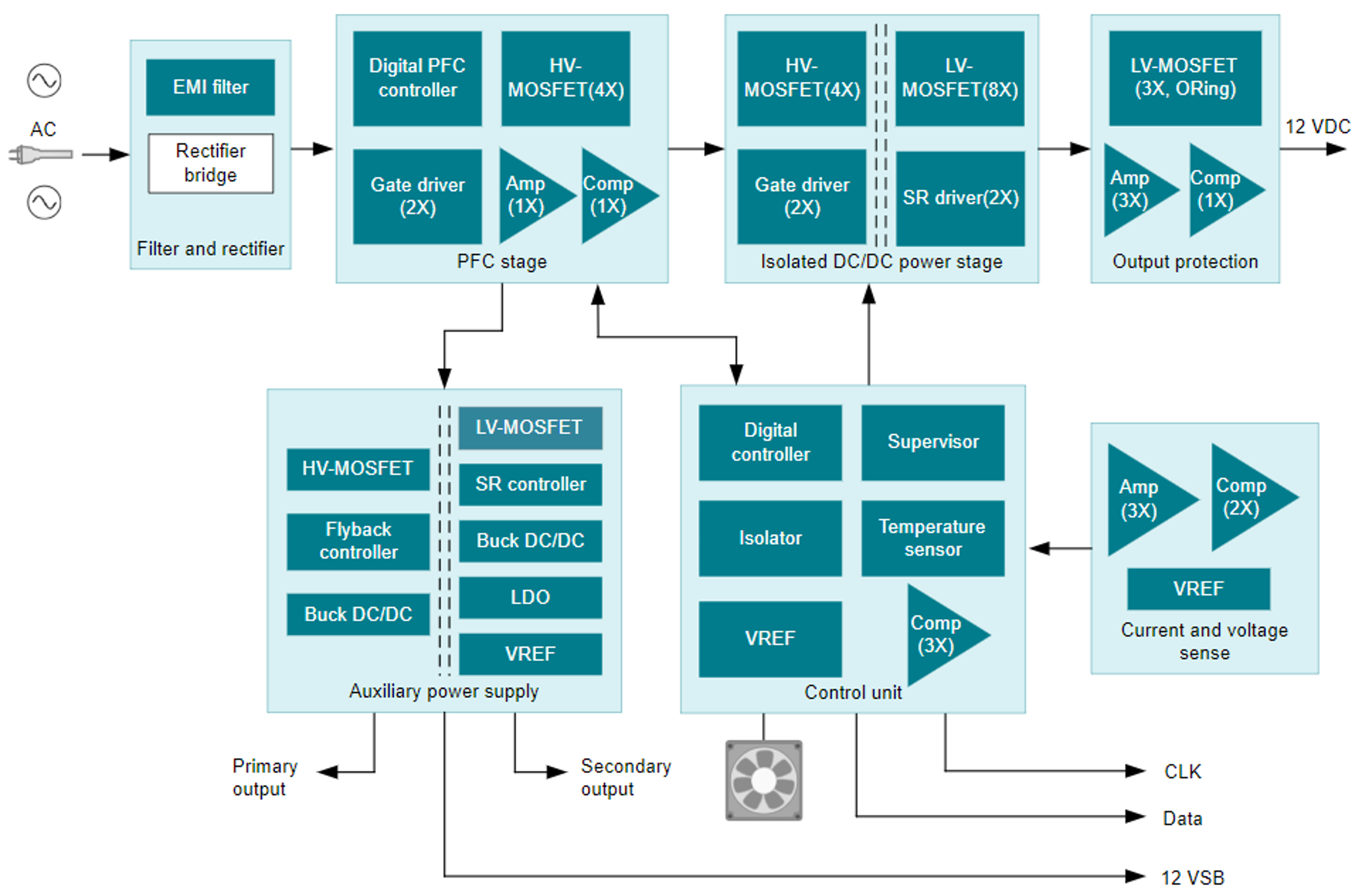
dummy loading still present even the main power off. As Figure 5-3 showing VDD for OPA and MCU or other analog IC and gate driver bias power, so
these extra loading still needs to be considered.
Customers can remove the output loading by disconnecting the diode at output winding, besides the main output with regulation feedback loop.
 Figure 5-1 VDD Charging Path
 Figure 5-2 Diode Reverse Current
 Figure 5-3 Server Block Diagram