SLUAAY3 September 2024 PCA9306 , TCA39306 , TCA9548A
2.1 What is the Hang Time Effect and Why Does the Hang Time Occur?
The hang time effect is defined in this application note as a length of time (typically nanoseconds) in which the I2C bus idles, hangs, before being fully pulled to a VOL typically during a HIGH to LOW bus transition. This can happen on a rising edge if the slew rate is fast enough. This effect is partially due to the passFET changing drain to source resistance, but is more directly caused by the parasitic capacitance on the I2C bus. Figure 2-4 shows the same example circuit as before using the TCA39306, but this time including parasitic bus capacitance CBUS1 and CBUS2.
 Figure 2-4 TCA39306 with Parasitic Bus Capacitance Included
If the target pulls SDA LOW, the voltage of CBUS2, which is the voltage at the drain or source of the passFET, can be pulled towards a VOL as shown in Figure 2-5.
 Figure 2-5 SDA2 is Pulled to a VOL with
CBUS2 Charged to 5.0V
Figure 2-5 SDA2 is Pulled to a VOL with
CBUS2 Charged to 5.0VThe output low voltage VOL defined in the I2C standard specifies the minimum LOW-level output current > 3mA at VOL = 0.4V. In this example, VOL is assumed to be near GND since the resistance of the open-drain driver is minimal.
As the target pulls LOW towards a VOL, the source voltage can decrease which can result in an increase in VGS quickly overcoming the threshold voltage of the passFET. This puts the passFET in a low impedance state connecting SDA1 to SDA2. The target can then see the charge on CBUS1 shown in Figure 2-6.
 Figure 2-6 PassFET Turns On Allowing Target to see Charge on CBUS1
This is exactly where the hang time effect occurs. SDA2 can resume being pulled to VOL only when the charge on parasitic bus capacitors CBUS1 and CBUS2 have been balanced, effectively hanging the I2C bus. Once both bus parasitic capacitance CBUS1 and CBUS2 are charge balanced, SDA2 can continue pulling LOW to VOL. SDA1 can follow SDA2, but SDA1 can be a RDS_ON voltage drop higher than SDA2 due to passFET ON resistance.
The amount of time the I2C bus hangs is dependent on several factors.
- Amount of parasitic bus capacitance in the system
- Voltage supply levels
- Which side initially pulls LOW with respect to largest bus capacitance
- Drive strength
When testing the TCA39306 for hang time, the phenomenon is unnoticeable at larger time scales. Figure 2-7 is the oscilloscope capture with address 0x74 being sent on SDA. Data is labeled appropriately for SDA1 (controller side) and SDA2 (target side). I2C is sent at 100kHz with 10kΩ pull up resistors on each side of the translator.
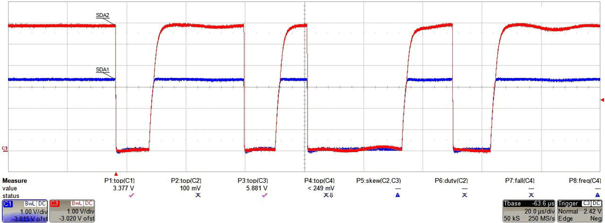 Figure 2-7 Address 0x74 Sent Across the TCA39306 when
VCC1 = 3.3V, VCC2 = 5.0V, CBUS1 = 100pF,
CBUS2 = 100pF, Pull LOW on Target Side (SDA2)
Figure 2-7 Address 0x74 Sent Across the TCA39306 when
VCC1 = 3.3V, VCC2 = 5.0V, CBUS1 = 100pF,
CBUS2 = 100pF, Pull LOW on Target Side (SDA2)When the time scale is changed to 50.0ns per division, the effect becomes more apparent Figure 2-8.
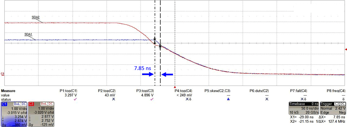 Figure 2-8 VCC1 = 3.3V, VCC2 =
5.0V, CBUS1 = CBUS2 = 100pF, Pull LOW on Target Side
(SDA2)
Figure 2-8 VCC1 = 3.3V, VCC2 =
5.0V, CBUS1 = CBUS2 = 100pF, Pull LOW on Target Side
(SDA2)Hang time has been measured to be 7.85ns in this test. The time that the bus hangs can be extended by adjusting the four parameters listed previously: parasitic bus capacitance, voltage supply levels, drive side, and drive strength. Drive strength can not be explored in this application note due to the inability to change this internally.
Changing the drive sides to the controller side (SDA1), hang time increases to approximately 36.25ns as in Figure 2-9.
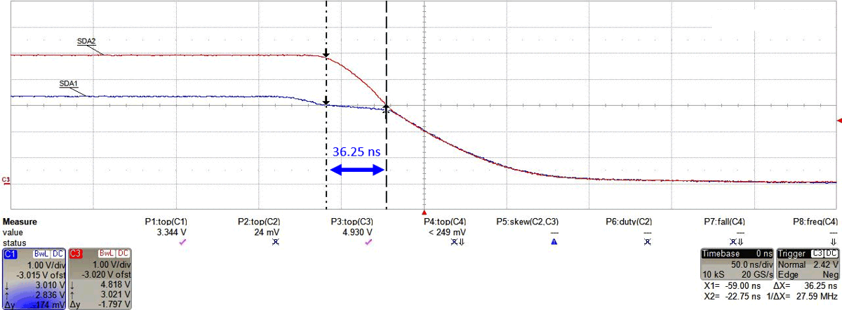 Figure 2-9 VCC1 = 3.3V, VCC2 =
5.0V, CBUS1 = CBUS2 = 100pF, Pull LOW on Controller Side
(SDA1)
Figure 2-9 VCC1 = 3.3V, VCC2 =
5.0V, CBUS1 = CBUS2 = 100pF, Pull LOW on Controller Side
(SDA1)Recalling the setup in Figure 2-6 the target’s bus capacitance CBUS2 is charged to 5.0V, while the controller’s bus capacitance CBUS1 is charged to 3.3V. An increase in hang time results in 7.85ns to 36.25ns between pulling LOW on target side vs. the controller side. Pulling LOW on the controller side results in larger hang time because a capacitor with larger voltage exists on the opposite end of the passFET. Once the passFET turns ON, the controller suddenly sees this 5.0V capacitor in which charge begins to flow. The target side pull LOW is quicker because the 5.0V capacitor is discharged first, leaving a 3.3V capacitor on the controller side to be discharged second.
Hang time becomes larger when parasitic bus capacitance is increased. This makes sense because a larger capacitor acts like a larger battery holding more charge. Consider a case where CBUS1 = 100pF and CBUS2 = 400pF. Rearrange the following equation for capacitance for voltage.
If capacitance is constant, an increase in voltage must also mean that the charge Q on the capacitor increases. Therefore, a
400pF capacitance charged to a potential of 5V can have more charge stored than a capacitor of 100pF charged to 5V. Both capacitors exhibit the same voltage, but more capacity for charge is present on the 400pF parasitic capacitor. Thus, when controller side (SDA1) is pulled LOW there can exist a lengthen period of hang time due to the larger amount of charge stored on the 400pF parasitic capacitor on the target side (SDA2) of the passFET. This holds the bus for a longer time before SDA reaches a VOL. Figure 2-10 captures this effect.
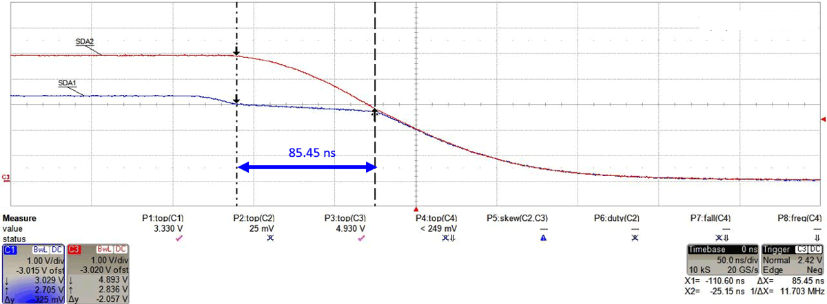 Figure 2-10 VCC1 = 3.3V, VCC2 =
5.0V, CBUS1 = 100pF, CBUS2 = 400pF, Pull LOW on Controller
Side (SDA1)
Figure 2-10 VCC1 = 3.3V, VCC2 =
5.0V, CBUS1 = 100pF, CBUS2 = 400pF, Pull LOW on Controller
Side (SDA1)Hang time increases to 85.45ns, more than double the amount in Figure 2-9. Hang time is made worse when the supply voltage of VCC2 is increased to 6.0V. An increased potential increases the total charge on CBUS2. Figure 2-11 shows extended hang time due to larger supply voltage on VCC2.
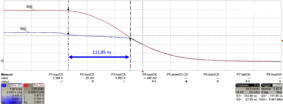 Figure 2-11 VCC1 = 3.3V, VCC2 =
6.0V, CBUS1 = 100pF, CBUS2 = 400pF, Pull LOW on Controller
Side (SDA1)