SLUSDE1E September 2018 – November 2024 UCC21540 , UCC21540A , UCC21541 , UCC21542
PRODUCTION DATA
- 1
- 1 Features
- 2 Applications
- 3 Description
- 4 Device Comparison Table
- 5 Pin Configuration and Functions
-
6 Specifications
- 6.1 Absolute Maximum Ratings
- 6.2 ESD Ratings
- 6.3 Recommended Operating Conditions
- 6.4 Thermal Information
- 6.5 Power Ratings
- 6.6 Insulation Specifications
- 6.7 Safety-Limiting Values
- 6.8 Electrical Characteristics
- 6.9 Switching Characteristics
- 6.10 Insulation Characteristics Curves
- 6.11 Typical Characteristics
- 7 Parameter Measurement Information
- 8 Detailed Description
-
9 Application and Implementation
- 9.1 Application Information
- 9.2
Typical Application
- 9.2.1 Design Requirements
- 9.2.2
Detailed Design Procedure
- 9.2.2.1 Designing INA/INB Input Filter
- 9.2.2.2 Select Dead Time Resistor and Capacitor
- 9.2.2.3 Select External Bootstrap Diode and Its Series Resistor
- 9.2.2.4 Gate Driver Output Resistor
- 9.2.2.5 Gate to Source Resistor Selection
- 9.2.2.6 Estimating Gate Driver Power Loss
- 9.2.2.7 Estimating Junction Temperature
- 9.2.2.8 Selecting VCCI, VDDA/B Capacitor
- 9.2.2.9 Application Circuits with Output Stage Negative Bias
- 9.2.3 Application Curves
- 10Power Supply Recommendations
- 11Layout
- 12Device and Documentation Support
- 13Revision History
- 14Mechanical, Packaging, and Orderable Information
7.5 Programmable Dead Time
UCC21542/A internally ties the deadtime circuit to VCCI, leaving pin 6 as not internally connected. This device always allows both outputs to overlap.
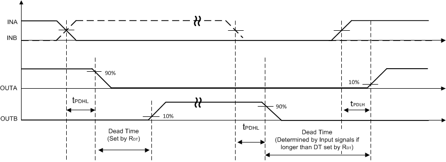
For UCC21540/A and UCC21541, tying DT to VCCI disables DT feature and allows the outputs to overlap. Placing a resistor (RDT) between DT and GND adjusts dead time according to the equation: DT (in ns) = 10 × RDT (in kΩ). TI recommends bypassing this pin with a ceramic capacitor, ≤1nF, close to DT pin to achieve better noise immunity. For more details on dead time, refer to Section 8.4.2.
 Figure 7-6 Dead Time Switching Parameters for UCC21540/A, UCC21541