SLUSDE1E September 2018 – November 2024 UCC21540 , UCC21540A , UCC21541 , UCC21542
PRODUCTION DATA
- 1
- 1 Features
- 2 Applications
- 3 Description
- 4 Device Comparison Table
- 5 Pin Configuration and Functions
-
6 Specifications
- 6.1 Absolute Maximum Ratings
- 6.2 ESD Ratings
- 6.3 Recommended Operating Conditions
- 6.4 Thermal Information
- 6.5 Power Ratings
- 6.6 Insulation Specifications
- 6.7 Safety-Limiting Values
- 6.8 Electrical Characteristics
- 6.9 Switching Characteristics
- 6.10 Insulation Characteristics Curves
- 6.11 Typical Characteristics
- 7 Parameter Measurement Information
- 8 Detailed Description
-
9 Application and Implementation
- 9.1 Application Information
- 9.2
Typical Application
- 9.2.1 Design Requirements
- 9.2.2
Detailed Design Procedure
- 9.2.2.1 Designing INA/INB Input Filter
- 9.2.2.2 Select Dead Time Resistor and Capacitor
- 9.2.2.3 Select External Bootstrap Diode and Its Series Resistor
- 9.2.2.4 Gate Driver Output Resistor
- 9.2.2.5 Gate to Source Resistor Selection
- 9.2.2.6 Estimating Gate Driver Power Loss
- 9.2.2.7 Estimating Junction Temperature
- 9.2.2.8 Selecting VCCI, VDDA/B Capacitor
- 9.2.2.9 Application Circuits with Output Stage Negative Bias
- 9.2.3 Application Curves
- 10Power Supply Recommendations
- 11Layout
- 12Device and Documentation Support
- 13Revision History
- 14Mechanical, Packaging, and Orderable Information
5.1 Pin Configuration and Functions
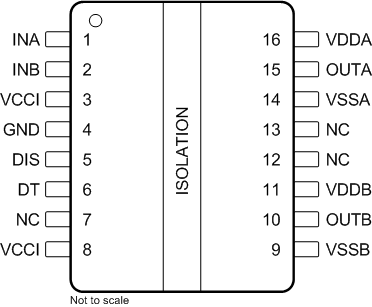
 Figure 5-1 DW Package16-Pin SOICTop View
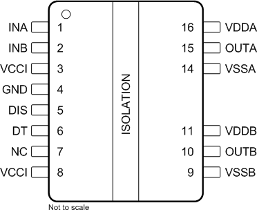
 Figure 5-2 DWK Package14-Pin SOICTop View
Table 5-1 Pin Functions
| PIN | TYPE (1) | DESCRIPTION | |
|---|---|---|---|
| NAME | NO. | ||
| DIS | 5 | I | Disables both driver outputs if asserted high, enables if set low. It is recommended to tie this pin to ground if not used to achieve better noise immunity. Bypass using a ≈ 1-nF low ESR/ESL capacitor close to DIS pin when connecting to a µC with distance. |
| DT | 6 | I | DT
pin configuration:
|
| GND | 4 | P | Primary-side ground reference. All signals in the primary side are referenced to this ground. |
| INA | 1 | I | Input signal for A channel. INA input has a TTL/CMOS compatible input threshold. This pin is pulled low internally if left open. It is recommended to tie this pin to ground if not used to achieve better noise immunity. |
| INB | 2 | I | Input signal for B channel. INB input has a TTL/CMOS compatible input threshold. This pin is pulled low internally if left open. It is recommended to tie this pin to ground if not used to achieve better noise immunity. |
| NC | 7 | — | No internal connection. This pin can be left floating, tied to VCCI, or tied to GND. |
| NC | 12 | — | No internal
connection. Recommended to leave floating for maximum creepage
from driver A to driver B as needed. For the SOIC-14 DWK Package, pin 12 and pin 13 are removed. |
| 13 | |||
| OUTA | 15 | O | Output of driver A. Connect to the gate of the A channel FET or IGBT. |
| OUTB | 10 | O | Output of driver B. Connect to the gate of the B channel FET or IGBT. |
| VCCI | 3 | P | Primary-side supply voltage. Locally decoupled to GND using a low ESR/ESL capacitor located as close to the device as possible. |
| VCCI | 8 | P | This pin is internally shorted to pin 3. Preference should be given to bypassing pin 3-4 instead of pins 8-4. |
| VDDA | 16 | P | Secondary-side power for driver A. Locally decoupled to VSSA using a low ESR/ESL capacitor located as close to the device as possible. |
| VDDB | 11 | P | Secondary-side power for driver B. Locally decoupled to VSSB using a low ESR/ESL capacitor located as close to the device as possible. |
| VSSA | 14 | P | Ground for secondary-side driver A. Ground reference for secondary side A channel. |
| VSSB | 9 | P | Ground for secondary-side driver B. Ground reference for secondary side B channel. |
(1) P = power, I = input, O = output