SLUU297B December   2007  – January 2022 TPS40195


  1.   Trademarks
  2. Introduction
  3. Description
    1. 2.1 Applications
    2. 2.2 Features
  4. TPS40195EVM Electrical Performance Specifications
  5. Schematic
    1. 4.1 Test Points
  6. Test Setup
    1. 5.1 Equipment
      1. 5.1.1 Voltage Source
      2. 5.1.2 Meters
      3. 5.1.3 Loads
      4. 5.1.4 Oscilloscope
      5. 5.1.5 Signal Generator
      6. 5.1.6 Recommended Wire Gauge
      7. 5.1.7 Other
    2. 5.2 Equipment Setup
  7. Test Procedure
    1. 6.1 Line and Load Regulation
    2. 6.2 Output Ripple Measurement (TP5, TP13)
    3. 6.3 Loop Analysis (TP7, TP8, TP10)
    4. 6.4 Disable (TP11) and Power Good (TP9)
    5. 6.5 Switch Node (TP4) and SYNC (TP12)
    6. 6.6 Equipment Shutdown
  8. TPS40195EVM Typical Performance Data and Characteristic Curves
    1. 7.1 Line and Load Regulation
    2. 7.2 Efficiency
    3. 7.3 Output Voltage Ripple
    4. 7.4 Transient Response
    5. 7.5 Bode Plots
    6. 7.6 Test Point Waveforms
  9. EVM Assembly Drawings and Layout
  10. List of Materials
  11. 10Revision History

EVM Assembly Drawings and Layout

The following figures (Figure 8-1 through Figure 8-3) show the design of the TPS40195EVM printed circuit board. The EVM has been designed using a 2-layer, 2-oz copper-clad circuit board with all components on the top side. Moving components to both sides of the PCB or using additional internal layers can offer additional size reduction for space constrained systems.
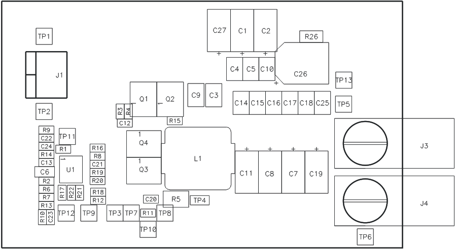
GUID-D2F65E2F-D490-4E7C-9C71-4ABE25B0DBA3-low.gifFigure 8-1 TPS40195EVM Component Placement (Viewed from Top)
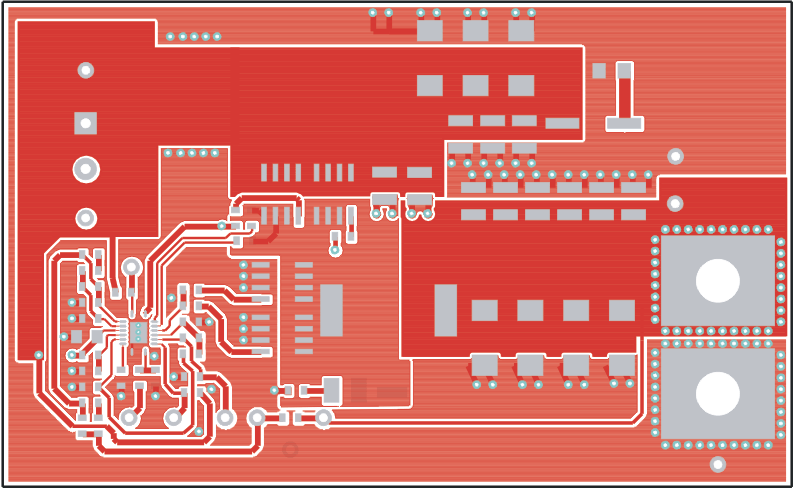
GUID-E65D6B9B-C61A-4F12-920C-1D66449039F2-low.gifFigure 8-2 TPS40195EVM Top Copper (Viewed from Top)
GUID-A6591DC5-2B31-487F-BE56-FA3254CBCDBB-low.gifFigure 8-3 TPS40195EVM Bottom Copper (X-ray Viewed from Top)