SLUU420A May   2010  – February 2022 TPS51217


  1.   Trademarks
  2. Description
    1. 1.1 Typical Applications
    2. 1.2 Features
  3. Electrical Performance Specifications
  4. Schematic
  5. Test Setup
    1. 4.1 Test Equipment
      1. 4.1.1 Voltage Source
      2. 4.1.2 Multimeters
      3. 4.1.3 Pulse Generator
      4. 4.1.4 Output Load
      5. 4.1.5 Oscilloscope
      6. 4.1.6 Fan
      7. 4.1.7 Recommended Wire Gauge
    2. 4.2 Recommended Test Setup
      1. 4.2.1 Input Connections
      2. 4.2.2 Output Connections
      3. 4.2.3 Other Connections
    3. 4.3 List of Test Points
  6. Test Procedure
    1. 5.1 Line/Load Regulation and Efficiency Measurement Procedure
    2. 5.2 Dynamic Output Voltage Transition Measurement Procedure
    3. 5.3 Equipment Shutdown
  7. Performance and Typical Characteristic Curves
    1. 6.1 Efficiency
    2. 6.2 Load Regulation
    3. 6.3 Line Regulation
    4. 6.4 Transient Response
    5. 6.5 Output Ripple
    6. 6.6 Switch-Node Voltage
    7. 6.7 Start and Stop
    8. 6.8 Dymamic Output Voltage Transitions
  8. EVM Assembly Drawing and PCB Layouts
  9. List of Materials
  10. References
  11. 10Revision History

EVM Assembly Drawing and PCB Layouts

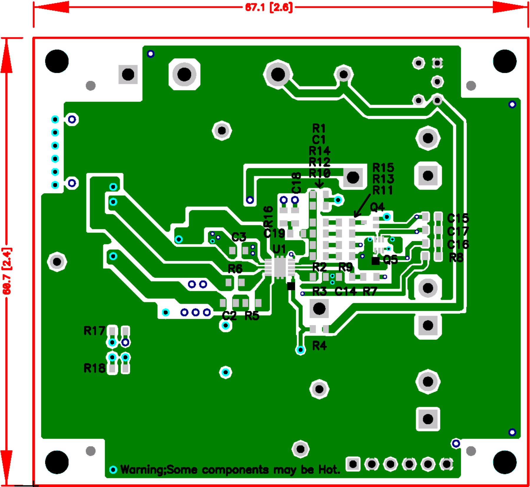
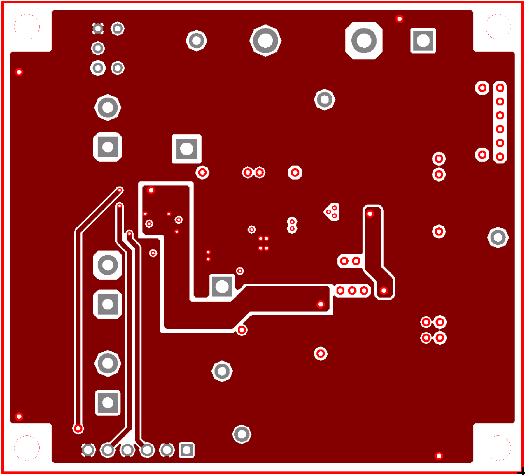
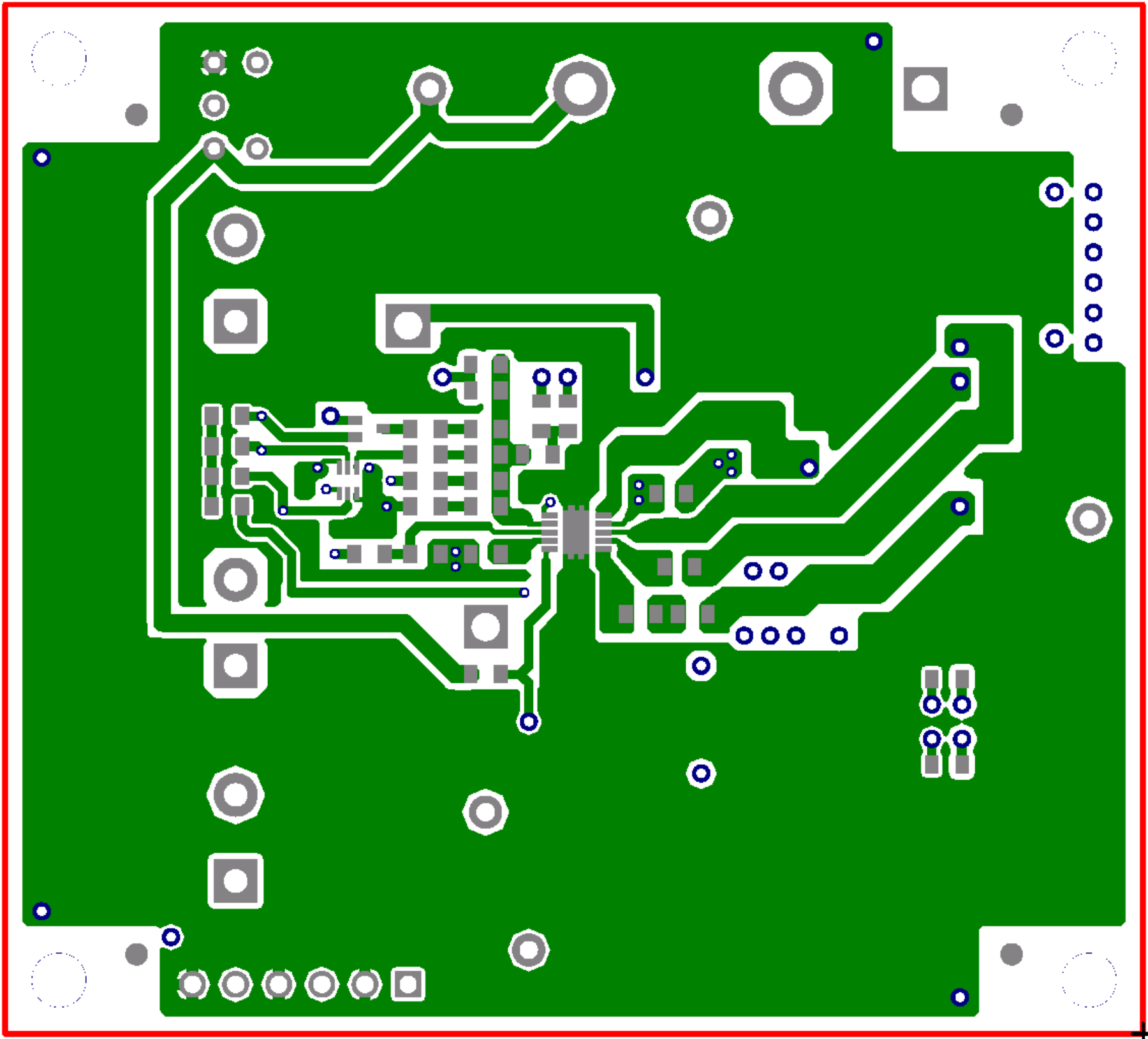
Figure 7-1 through Figure 7-6 show the design of the TPS51217EVM-533 printed circuit board. The EVM has been designed using four layers, of 2-oz. copper circuit board.

GUID-CDA4EAF5-2059-437E-A6CD-83CC9237F7D7-low.gifFigure 7-1 Top Layer Assembly Drawing (Top View)
GUID-3F1353A2-207F-4E3D-A860-9E7E536DDF07-low.pngFigure 7-3 Top Copper (Top View)
GUID-C07F9592-FF39-4287-9899-07E8D5DE4677-low.pngFigure 7-2 Bottom Assembly Drawing (Bottom View)
GUID-F1E83D44-1410-43AF-92BB-F242BE3F8B40-low.pngFigure 7-4 Internal Layer 1 (Top View)
GUID-7E81480D-7A56-4909-A28A-A2F3A56FBB2E-low.pngFigure 7-5 Internal Layer 2 (Top View)
GUID-D0686623-A907-407C-9D6F-F0A171FA5FAD-low.pngFigure 7-6 Bottom Copper (Top View)