SLUUC04A February 2019 – June 2021 TPS568230
4 Board Layout
This section provides a description of the TPS568230EVM board layout and layer illustrations. The board layout for the TPS568230EVM is shown in below figures. The top-side layer of the EVM is laid out in a manner typical of a user application. The top and bottom layers are 2-oz copper, and internal layers are 1-oz copper.
The top layer contains the main power traces for VIN, VOUT, and SW. Also on the top layer are connections for the remaining pins of the TPS568230 and the majority of the signal traces. There is a large area filled with ground. The internal layer-1 and layer-2 are ground plane. The bottom layer is another ground plane with some additional signal. The top-side ground traces are connected to the bottom and internal ground planes with multiple vias placed around the board.
The input decoupling capacitors and bootstrap capacitor are all located as close to the IC as possible. Additionally, the voltage set point resistor divider components are kept close to the IC. The voltage divider network ties to the output voltage at the point of regulation. For the TPS568230, an additional input bulk capacitor may be required, depending on the EVM connection to the input supply. Critical analog circuits such as the voltage set point divider, EN resistor, SS capacitor, MODE resistor, and AGND pin are terminated to quiet analog ground island.
 Figure 4-1 Component Placements
 Figure 4-2 Top Layer
 Figure 4-3 Internal Layer1
 Figure 4-4 Internal Layer2
 Figure 4-5 Bottom Layer
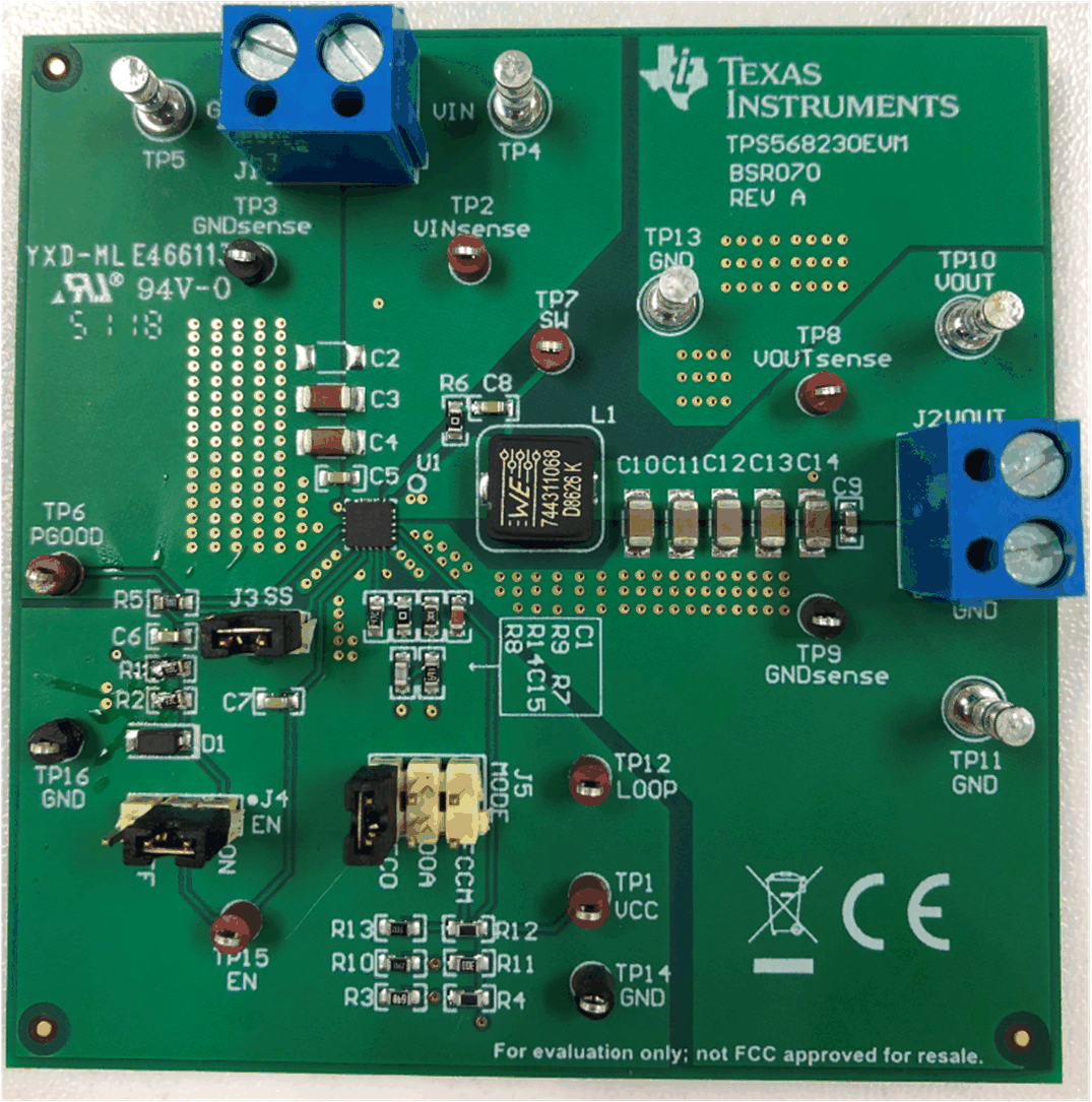
Figure 4-6 and Figure 4-7 are high revolution images of the EVM board.
 Figure 4-6 EVM Front View
 Figure 4-7 EVM Back View