SLUUC47A December   2019  – August 2021 TPS546D24A


  1.   Trademarks
  2. Description
    1. 1.1 Before You Begin
    2. 1.2 Typical Applications
    3. 1.3 Features
  3. Electrical Performance Specifications
  4. Schematic
  5. Test Setup
    1. 4.1 Test and Configuration Software
      1. 4.1.1 Description
      2. 4.1.2 Features
    2. 4.2 Test Equipment
      1. 4.2.1 Voltage Source
      2. 4.2.2 Multimeters
      3. 4.2.3 Output Load:
      4. 4.2.4 Oscilloscope
      5. 4.2.5 Fan:
      6. 4.2.6 USB-to-GPIO Interface Adapter:
      7. 4.2.7 Recommended Wire Gauge
    3. 4.3 Tip and Barrel Measurement
    4. 4.4 List of Test Points, Jumpers, and Connectors
    5. 4.5 Evaluating Single Phase Operation
    6. 4.6 Evaluating Split Rail Input
    7. 4.7 Configuring EVM to Overdrive VDD5
  6. EVM Configuration Using the Fusion GUI
    1. 5.1 Configuration Procedure
  7. Test Procedure
    1. 6.1 Line and Load Regulation and Efficiency Measurement Procedure
    2. 6.2 Efficiency Measurement Test Points
    3. 6.3 Control Loop Gain and Phase Measurement Procedure
  8. Performance Data and Typical Characteristic Curves
    1. 7.1  Efficiency
    2. 7.2  Load and Line Regulation (Measured Between TP22 and TP25)
    3. 7.3  Transient Response
    4. 7.4  Control Loop Bode Plot
    5. 7.5  Output Ripple
    6. 7.6  Power MOSFET Drain-Source Voltage
    7. 7.7  Control On
    8. 7.8  Control Off
    9. 7.9  Control On With Pre-biased Output
    10. 7.10 Current Sharing Between Two Phases
    11. 7.11 Thermal Image
  9. EVM Assembly Drawing and PCB Layout
  10. Bill of Materials
  11. 10Using the Fusion GUI
    1. 10.1  Opening the Fusion GUI
    2. 10.2  General Settings
    3. 10.3  Changing ON_OFF_CONFIG
    4. 10.4  Pop-up for Some Commands While Conversion is Enabled
    5. 10.5  SMBALERT# Mask
    6. 10.6  Device Info
    7. 10.7  Phase Commands
    8. 10.8  All Config
    9. 10.9  Pin Strapping
    10. 10.10 Monitor
    11. 10.11 Status
  12. 11Revision History

Power MOSFET Drain-Source Voltage

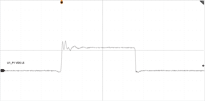
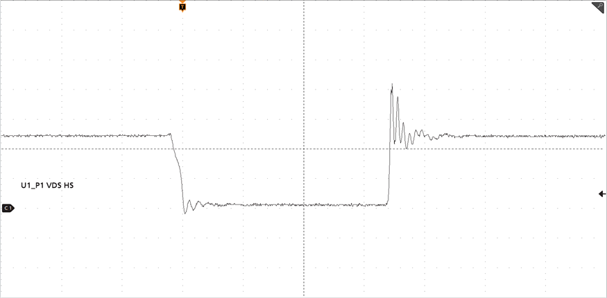
Figure 7-9 and Figure 7-10 show the low-side and high-side MOSFET drain-source voltage (VDS) at 80-A load. The voltage is measured with 1-GHz bandwidth and at the solder mask openings near the U1_P1 IC using a 1-GHz differential probe.
GUID-3E443987-9C6F-441F-BC91-C51B60787A78-low.gif
Timescale = 40 ns/div, CH1 = Low-side VDS at 5 V/div
Figure 7-9 Low-side MOSFET VDS
GUID-8C0D4159-0175-4750-83BE-F549D03DFF84-low.gif
Timescale = 40 ns/div, CH1 = High-side VDS at 5 V/div
Figure 7-10 High-side MOSFET VDS