SLUUC68A August 2020 – April 2021 TPS563207
5.1 Layout
The board layout for the TPS563207EVM is shown in Figure 5-1, Figure 5-2, and Figure 5-3. The top layer contains the main power traces for VIN, VOUT, and ground. The top layer also has the connections for the pins of the TPS563207 and a large area filled with ground. Most of the signal traces are also located on the top side. The input decoupling capacitors, C2, C3, and C4 are located as close to the IC as possible. The input and output connectors, test points, and all of the components are located on the top side. The bottom layer is a ground plane along with the switching node copper fill, signal ground copper fill and the feed back trace from the point of regulation to the top of the resistor divider network. Both the top layer and bottom layer use 2-oz. copper thickness.
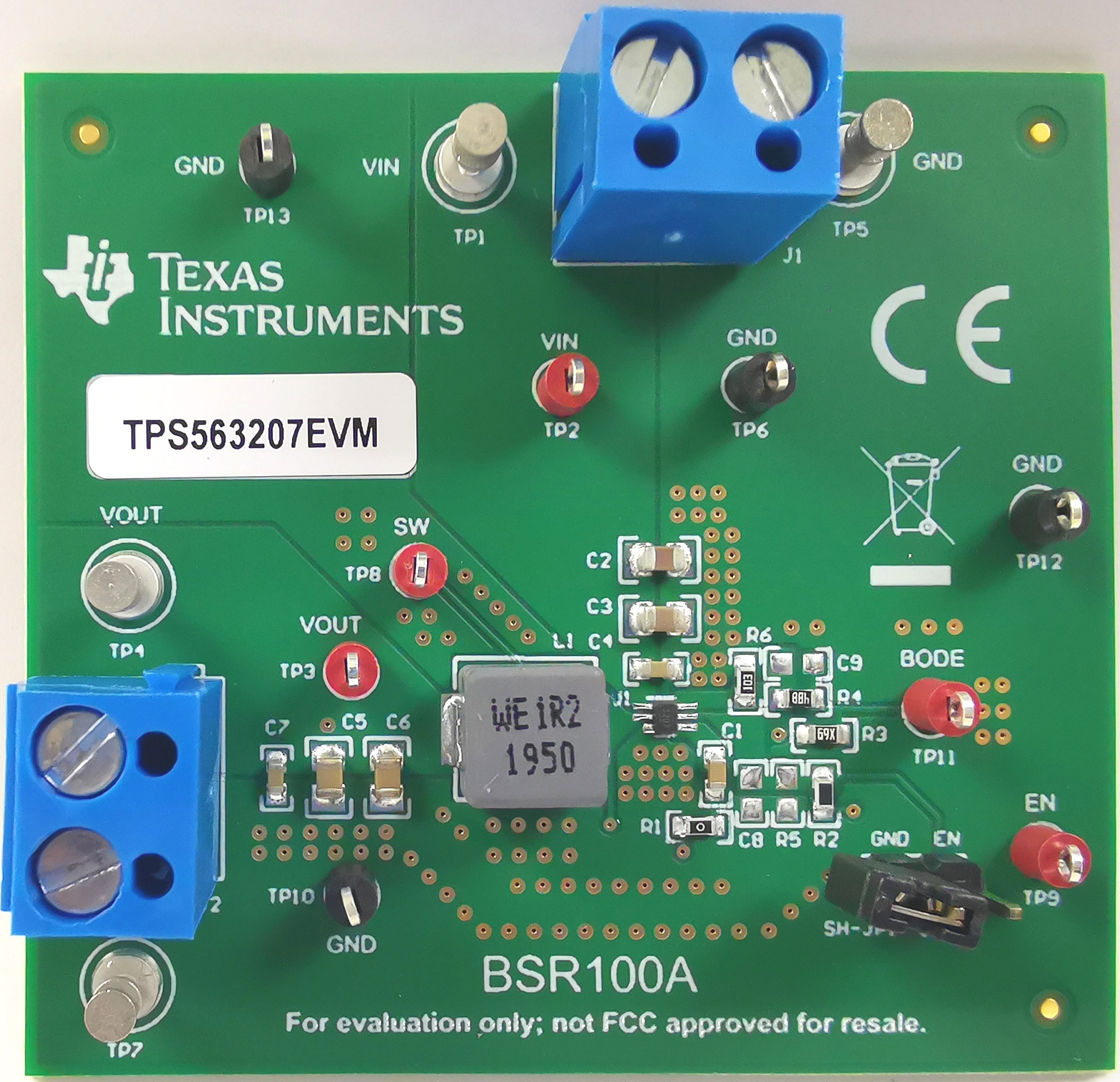
Figure 5-4 and Figure 5-5 are the TPS563207EVM top view and bottom view, respectively.
 Figure 5-1 TPS563207EVM Top
Assembly
 Figure 5-2 TPS563207EVM Top
Layer
 Figure 5-3 TPS563207EVM
Bottom Layer
 Figure 5-4 TPS563207EVM
Board Top View
 Figure 5-5 TPS563207EVM
Board Bottom View