SLUUCV0B August   2023  – April 2024 TPSM8287A06 , TPSM8287A10 , TPSM8287A12 , TPSM8287A15


  1.   1
  2.   Description
  3.   Features
  4.   4
  5. 1Evaluation Module Overview
    1. 1.1 Introduction
    2. 1.2 Kit Contents
    3. 1.3 Specification
    4. 1.4 Device Information
  6. 2Hardware
    1. 2.1 Safety Instructions
    2. 2.2 Header Information
    3. 2.3 Jumper Information
    4. 2.4 Interfaces
    5. 2.5 Test Points
  7. 3Software
  8. 4Implementation Results
    1. 4.1 Evaluation Setup
      1. 4.1.1 Ripple Measurement Setup
      2. 4.1.2 Operation With Output Voltages Above 2V
      3. 4.1.3 Loop Response Measurement
      4. 4.1.4 Precise Turn-on Voltage
    2. 4.2 Performance Data and Results
  9. 5Hardware Design Files
    1. 5.1 Schematics
    2. 5.2 PCB Layouts
    3. 5.3 Bill of Materials (BOM)
  10. 6Additional Information
    1. 6.1 Trademarks
  11. 7Revision History

Schematics

Figure 6-9, Figure 6-2, Figure 6-11, and Figure 6-4 show the EVM schematics.

The TPSM8287A06BASEVM uses the TPSM8287A06BASRDVR IC.

The TPSM8287A12BBSEVM uses the TPSM8287A12BBSRDVR IC.

The TPSM8287A10BAHEVM uses the TPSM8287A10BAHRDWR IC.

The TPSM8287A15BBHEVM uses the TPSM8287A15BBHRDWR IC.
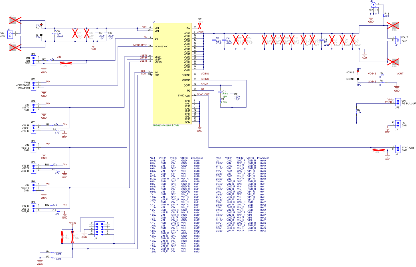
GUID-20231027-SS0I-CRZJ-CBJF-SJZ702KDQJ74-low.gifFigure 5-1 TPSM8287A06BASEVM Schematic
GUID-20230628-SS0I-CGF8-GF3D-SFVSBGTVGPDP-low.svgFigure 5-2 TPSM8287A12BBSEVM Schematic
GUID-20240214-SS0I-BDCH-GNNP-WXNNVBSKKWTD-low.svg Figure 5-3 TPSM8287A10BAHEVM Schematic
GUID-20240214-SS0I-HLGW-CRPC-LQQ7VTZK6FMF-low.svg Figure 5-4 TPSM8287A15BBHEVM Schematic