SLVA275C january 2010 – may 2023 UCD9081
- Abstract
- Trademarks
- 1Introduction
- 2Hardware
- 3Software
-
4User Configuration
- 4.1 Configuration Parameter Memory Map
- 4.2
Configuration Parameter Detail
- 4.2.1 GpDir
- 4.2.2 NegateEnablePolarity
- 4.2.3 SeqEventPending
- 4.2.4 SequenceEventParameters
- 4.2.5 SequenceEventLink
- 4.2.6 SequenceEventData
- 4.2.7 DependencyMasks
- 4.2.8 UnderVoltageThresholds
- 4.2.9 OverVoltageThresholds
- 4.2.10 RampTime
- 4.2.11 OutOfRegulationWidth
- 4.2.12 UnsequenceTime
- 4.2.13 EnablePolarity
- 4.2.14 SaveRailLog
- 4.2.15 ReferenceSelect
- 4.2.16 LastUnusedSeq
- 4.2.17 IgnoreGlitchAlarms
- 4.2.18 IgnoreFlashErrorLog
- 4.2.19 Checksum
- 5Additional Considerations
- 6References
- 7Revision History
5.2.1 UCD9081 Startup
I2C communication with the UCD9081 cannot be established immediately after power is applied. On power up, the UCD9081 performs several operations on the contents of the user parameter section. A RESET delay is incurred during this operation, and the digital I/O pins are in a high-impedance state. At the end of this operation, the sequencer application starts and I2C communication may commence.
The startup delay can vary based on the cases that follow;
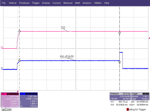
- Normal case: The UCD9081 performs a checksum test on the contents of the user parameter section. If the test passes, then the UCD9081 compares the contents of the user parameters section to the contents of the application (or last-known-good configuration) parameters section to see if the parameters have changed. If the two areas match, then the sequencer application starts. This nominally takes 35 ms as shown in Figure 5-1
 Figure 5-1 Power-Up Delay, no Parameter Change
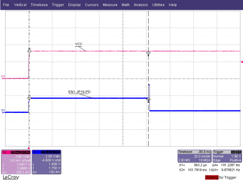
 - Configuration change-pass checksum case: If the user parameter area has been updated but the device has not been RESET (see UCD9081 data sheet RESET description) then the user and application parameter areas do not match. After the next RESET, the checksum test occurs. If the test passes, then the UCD9081 copies the user parameters to the application parameters area. This nominally takes 102 ms as shown in Figure 5-2. Subsequent power ups (with unchanged user parameters) fall into the normal category.
- Configuration change-fail checksum case: If the checksum test fails, then the UCD9081 copies the application parameters back to the user parameters area. This nominally takes 102 ms as shown in Figure 5-2.
 Figure 5-2 Power-Up Delay, With Parameter Change