SLVA514C July 2014 – November 2022 TPS62125
2.2 Enable Hysteresis Pin
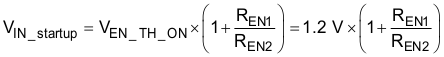
The enable comparator typically has a built-in hysteresis of 50 mV. This hysteresis can be increased with an external resistor divider connected to the EN_hys pin. The equations to calculate the external resistor values for a buck converter are located in the applications section of the data sheet (Equations 6–10). Because the device is now an inverting buck-boost converter, the equations must be modified to account for VOUT, which is the GND terminal of the device. The VEN_TH_ON variable remains the same since there is usually no negative output voltage when the part is enabled. The equations for the inverting buck-boost topology are:

In order for the VIN_stop threshold to operate, VIN_startup must be greater than VIN_stop - VOUT, where VOUT is a negative value.
If the EN_hys pin is not being used to adjust the hysteresis, it can instead be used to provide an output discharge path (explained in Section 2.4).