SLVA888C April 2017 – January 2021 TPS65987D , TPS65988
- Trademarks
- 1Schematic Design Guidelines
- 2Layout Guidelines
- 3Summary
- 4References
- A Appendix
- Revision History
2.2 Hi Speed Lines
In a USB PD system, hi speed signals can reach up to 10 Gbit/s. In a Thunderbolt 3 based system, the data rate can rise to 40 Gbit/s. At high data rates, signal integrity may not be maintained. Use these guidelines to avoid signal quality issues.
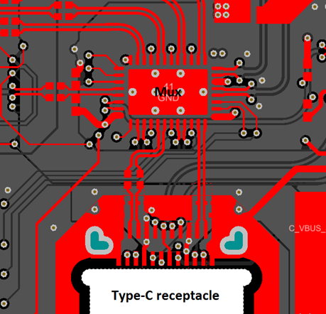
- Ensure SuperSpeed or Alternate Mode multiplexers are placed close to the Type-C receptacle. This is required to avoid signal quality issues as the high speed lines can directly be routed to the multiplexer.
 Figure 2-1 High Speed Signal Routing Example
 - Do not place switching circuits close to the multiplexer and the high speed signal traces to avoid noise coupling in these signals.
- Maintain 90-Ω differential impedance for high speed signals.
- Two differential pairs must be separated by at least three times the width of the differential pair and should be uniformly laid out.
- Intra Pair length of the differential pair traces should be matched within 5 mills.
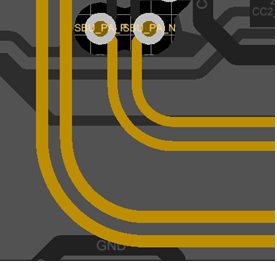
- Avoid bents on high speed signals. If required, then use curved bents or 45° bents. Never use 90° bent.
 Figure 2-2 Recommended Signal Bents
 - If two pairs of high speed signals cross each other on two planes, then there must be a ground plane between these two planes.
- Maintain continuous grounding while changing the layer of high speed signal to ensure uniform impedance. When placing a via on a high speed signal, place GND vias next to them to maintain uniform impedance.